Abstract
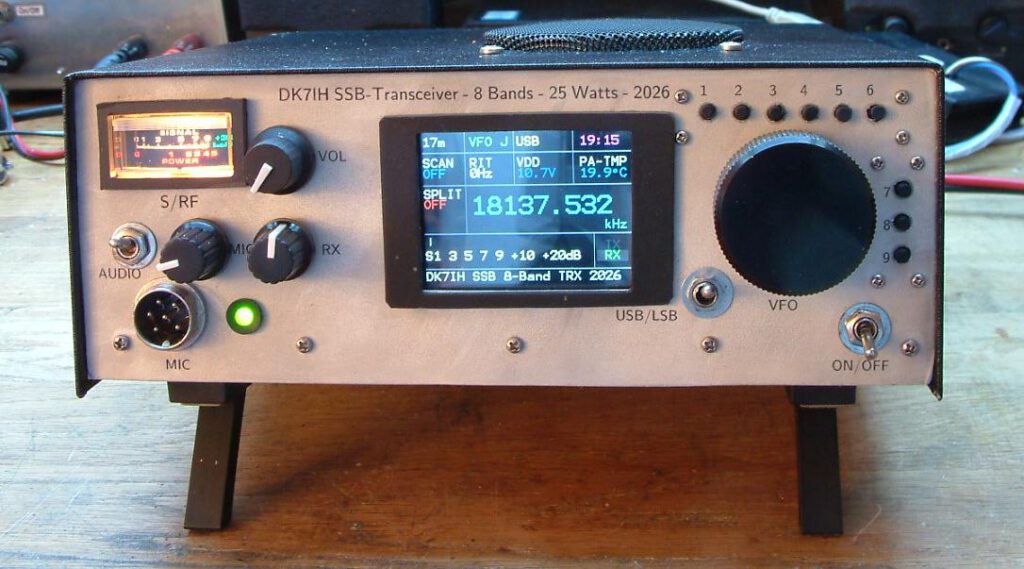
This article refers to a compact SSB radio designed for outdoor usage like SOTA/POTA activities etc. The output power is limited to 25 Watts PEP on all bands to ensure longer operation periods using moderate size batteries. The design covers the 3.5, 5.3, 7, 14, 18, 21, 24, and 28 MHz bands. USB and LSB are available as modulation types on all bands.
The radio frequency stages in this radio follow traditional analog design whereas frequency generation for the VFO signal is performed by a 14-bit Direct Digital Synthesizer, the AD9951 IC supplied by Analog Devices. In a later version of this radio this applies also to the Local Oscillator (LO) that has been replaced by the same DDS chip.
The microcontroller (MCU) to controll all the digital stuff is an STM32F411 by STMicroelectronics on the respective breakout board (named as “Black Pill board“). Also integrated is a Real Time Clock (RTC) for operators who prefer standard paper based QSO logging in the field without the necessity to carry a smartphone or a laptop computer. Also an EEPROM module is included to store user preferences. Eight user accessible keys allow controlling the functions in the radio without any menu based user interface.
Weight of the radio is about 1.4 kg, cabinet dimensions are 20 x 20 x 7 centimeters.
Details
Main modules
This transceiver is made up of 6 main sections that are divided again into subsections to keep the design highly modular. These main sections are:
- The MCU board, VFO and Local Oscillator (LO),
- Receiver,
- SSB Generator,
- Power Transmitter,
- Final Low Pass Filter,
- T/R Switching.
Also there are some sub-sections (e. g. DC decoupling networks to improve performance in the transmitter).
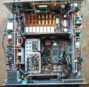
1. The MCU Board
This board controls the VFO, the LCD, the user interface and reads analog values from different sensors.
The schematic:
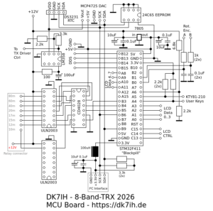
The MCU, the STM32F411 microntroller, is mounted to a breakout board, the widely known “Blackpill” board. surrounded by various circuits.
LCD
We use a colored LCD display here, an ILI9341 type. This LCD can be driver by various techniques (SPI, parallel). We have chosen the parallel mode. This makes sure that there is a very fast image display and the screen does not have any visible latency. These parallel displays are offered using 8 or 16 data bus width. To make wiring easier the 8-bit version has been chosen. It means that there are 3 control lines (RES, RS, WR) and 8 data lines (D7:D0).
In a later version I have gone back to a 4×20 Line LCD (EA205B-6NLW).
Band relay driving
Switching the bands in this unit is performed by signal relays. This is to maintain maximum decoupling of the various signal paths to a maximum degree. For driving 8 relays 3 output pins are used. They drive a CD4028 (a BCD-to-decimal converter). The 8 output lines from this IC are fed into the relay driver ICs, the ULN 2003, basically a DC motor driver. This IC uses open collector circuit together with integrated clamp diodes which makes it ideal as a low-fuss relay driver.
EEPROM
As the STM32F4xx controller family does not contain an EEPROM chip, the user data is stored in an 24C65 EEPROM IC that is addressed and data-supplied via the I2C bus.
TX driver control
One central problem in designing a multi band HF radio is the unequal gain distribution over the full band width. As this radio spans 3 frequency octaves and amplifier gain in RF amplifiers usually is doubled each octave down to the lower end of the spectrum we can imagine that the frequency -> gain function might be a problem. One onset to cope with this issue could be using an ALC control and therefore some sort of negative feedback over the whole transmitter chain. An alternative is to set fixed control voltage for each band and drive the transmitter respectively. Together with a microphone compressor/limiter this should work as well. With this idea the transmitter’s drive is adjusted individually for each band by the designer, stored as a numeric value into the EEPROM in the digital section and then being recalled and set each time the respective band is accessed.
The hardware used to achieve this goal is a MCP4725 digital-2-analog (DAC) converter, an IC that is also I2C bus controlled.
Analog data
The STM32F411 includes also a 12 bit analog-2-digital converter (ADC). This unit is used to measure final PA temperature (using a KTY81-210 PTC), the current supply voltage (VDD) via a voltage divider, the receiver’s AGC voltage for S-Meter indication and the rectified RF power provided by the final PA when on transmit. The 2 latter data are also displayed by an analog instrument.
VFO
The AD9951 based DDS VFO has been mounted to a separate PCB. supply voltage is 5V derived from the MCU board.
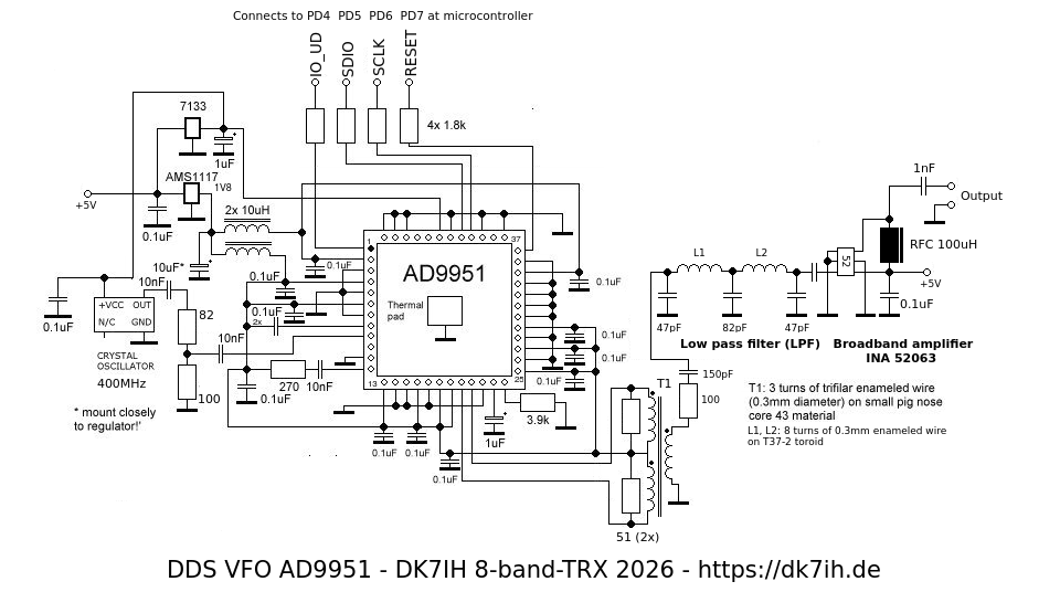
The clock rate applied is 400MHz to ensure maximum signal quality. We use the synthesizer’s balanced output (T1, a trifilar broadband transformer) for higher output voltage compared to a single ended design. A broadband amplifier (INA 52063 by Hewlett Packard) shifts output level to about 1.5Vpp over the full frequency range (13 to 39 MHz) and beyond.
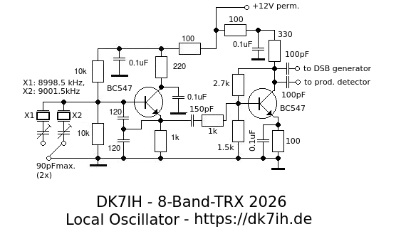
Local Oscillator
A simple analog draft has been chosen. Sideband switching is performed by a single switch between the two crystals.
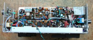
2. The Receiver
The basic concept is a single conversion superhet (9 MHz interfrequency) with a radio frequency preamplfier, a passive balanced diode ring mixer + one amplifier stage to compensate for conversion loss in the passive mixer layout, a two stage interfrequency amplifier, a NE612-based product detector, an audio derived AGC, a bipolar audio preamplifier and a TBA820M final audio amplifier stage.
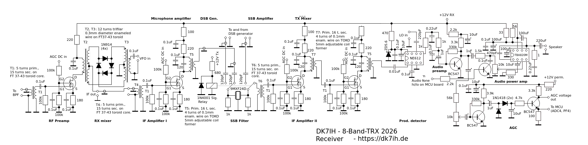
As we can learn from the schematic all RF and IF based amplifier are equipped with Dualgate-MOSFETS. Here we can use NOS (new old stock) types like the 40673, more modern types like the BF 900 or SMD types like the BF998 (mounted to a breakout board in case the radio is built in through-hole technology).
One main advantage of this design is, that dual gate MOSFETs provide comparatively better noise figure compared to BJTs which helps improving signal reception on the higher bands. As all these 4 amplifier stages are also integrated into AGC chain a high level of gain variation by the AGC is ensured. The passive diode ring mixer on the other hand is not prone on being easily overrun by high signal levels on the lower bands. Thus even with antennas delivering high energy there are no detectable “ghost” signals in the audio.
The SSB filter is shared between the transmit and the receive branch in the radio, the switching between transmit and receive mode also is managed using small signal relays.
For the purpose of impedance matching toroidal transformers have been put in between the various RF and IF stages.
3. SSB Generator
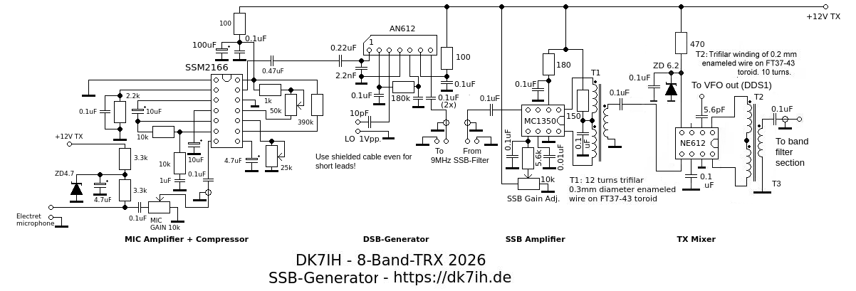
This unit consists of the microphone amplifier that also contains a compressor/limiter device (IC is SSM2166), the DSB modulator (AN612), the SSB filter (shared between TX and RX) and the SSB amplifier (MC1350 manually gain controlled).
The SSM2166 usually has 4 variable resistors to control its audio performance of which we use only 2. The first one is the “Noise Gate Set” that defines the level where the audio input is shut down when signal is too low. This function can be accessed via a variable resistor to pin 9. Connected to pin 10 we see the “COMP RATIO SET” which defines the compression ratio. A potentiometer or resistor to ground sets the compression ratio. 0Ω in the potentiometer is equivalent to “no compression”, higher resistance increases compression up to 1 by 15. Gain ist set via pin 2, here a fixed resistor has been tested to provide sufficient gain by a connected electret microphone.
The DSB generator we use is a AN612, known from many SSB CB radios of the 1980s and 1990s. It supplies high carrier suppression (up to >50dB). A balancer pot has been integrated to optimize this setting.
After the DSB signal has been fed through the SBB Filter, a commercial 4-pole 9MHz filter by box73.de, the signal is amplified by the video amplifier IC MC1350. Gain adjustment is done by using a 5k potentiometer to set output level in an way that signal does not overdrive the transmit mixer.
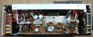
4 Power transmitter
 4 Power transmitter
- Negative feedback between collector and base, and
- Emitter degeneration.
- Impedance matching between two stages
- DC decoupling between the single stages
Impedance matching
- Resistive load (R)
- Inductive Reactance (XL)
- Capacitive Reactance (XC)
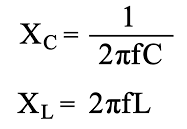
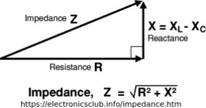
.As Z is defined as the Hypotenuses in a rectangular triangle sometimes complex numbers are applied to show the math behind this idea:
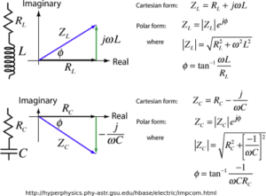
Explaining this to a fully extent would lead much too far when discussion matching problems in our transceiver. But we can say that impedance is a physical quantity that is highly frequency dependent and depending on the Ls and Cs involved in an AC circuit.
In general we can deduce that with high power RF amplifiers we can give the following statements:
- Input impedance is always higher than output impedance in a single amplifier stage.
- From stage to stage, as current rises, impedance is lower in stages that handle higher power levels than in those that amplify low power levels.
Thus impedance matches between stages is essential as with impedance the transmitter loses gain, distortion will be higher and signal quality will be lower than in cases where a good impedance matching has been integrated. Above this a significant part of RF energy is reflected into the source from the load.
Basically there are 2 general ways to optimize impedance matching between the stages:
- Broadband RF transformers
- PI or L networks
In broadband transformers we usually have a primary and a secondary winding. According to the Law of conservation of Energy and as Power (P) is defined as the product of Current (I) and Voltage (V) as P = V * I we can calculate that as voltage rises the amount of current must decrease by the same ratio. As R is defined as the fraction of V over I we can see that with a winding ration of 2 by 1 the impedance will decrease by a ratio of 4 (2²).
Broadband transformers require core materials that maintain high permeability and low losses across a wide frequency spectrum. For RF use between 3 and 30 MHz the material called “43” has proven to match these requirements. In low-power stages we mainly use toroids, in high-power stages “pig-nose” cores are applied as they can stand higher magnetic flux without being prone to saturation.
PI-networks
As impedance matching is, among other factor, depending on the frequency, a Pi-Network has been introduced to optimize impedance matching between driver and final transmitter stage. Detailed circuit is given in the schematic, here is the data for the filter:
DC decoupling
Sometime when testing the transmitter strange readings can be observed on the oscilloscope. The dual-tone signal does not appear to be of constant peak power but goes up and down with a rate of about 2 to 4 oscillations per second. This usually comes from low frequency coupling over the DC +12V lines. To avoid this large electrolytic capacitors have been integrated into the high power RF stages as well as coils for high current working as low pass filters.
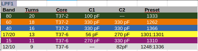
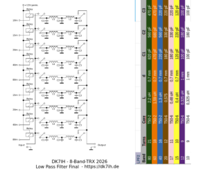
5 Final Low Pass Filter
As this transceiver has been designed for 8 individual frequency band, 8 different low pass filters were integrated to optimize impedance matching and harmonic filtering in the output section of the radio. To simplify the design it also would have been possible to use one filter for two neighboring frequencies. But as there has been sufficient space in the cabinet, 8 different filters have been constructed.
The filter section is designed to handle power levels of up to 30 watts PEP using T50-2 and T50-6 cores and capacitors rated for 120V max. voltage.
6 Transmit/Receive Switching
As in the previous design a relay-less idea has been used. Two p-channel power MOSFETs switch either the transmit or the receive branch in the DC supply chain.
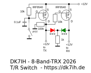
The IRF9540 as a p-channel MOSFET conducts between Source and Drain when Gate is tied to GND. When the PTT is pushed, the Gate pin of the TX MOSFET is pulled to GND leading to current between Drain and Source. As Drain now is positive, the Gate of the RX MOSFET is pulled “high”, so this MOSFET shows high resistance and cuts of the DC from the receiver.
Within the power RF amplifiers (driver and final) the collectors of the drive and the final amplifier stages are connected permanently to +12 V to avoid their high currents running through the MOSFETs in this switch unit. Only bias current is applied when the radio goes “on air” thus shifting the RF power transistors into operational mode.
Performance Examples
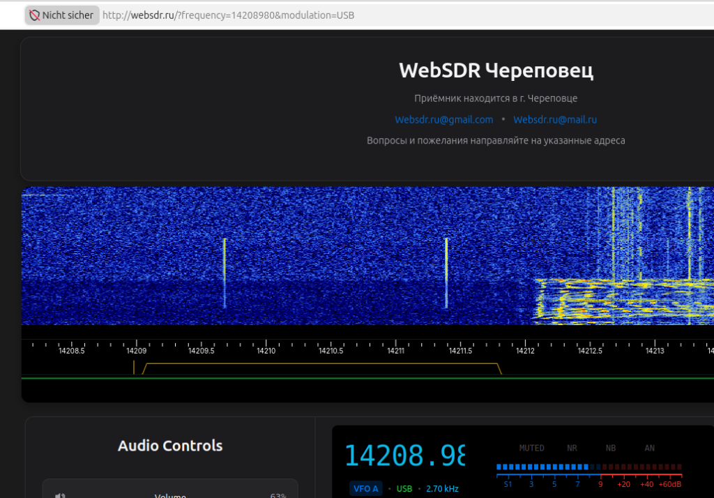
The picture shows an output sample of a dual-tone signal on the 14MHz band. The Vpp reading of 105V to 50Ω impedance results in a PEP output power of 25+ Watts.

The same signal picked up on a Russian WebSDR:
Thank you so much for watching and 73!
Peter (DK7IH)
(This text has not been AI generated nor translated by a machine.)