Hi again! This project directly “beams” you back to the “Good ol’ 80s” when there was no stuff like “DDS, “OLED” or even “SDR” or other modern technology we today use to build our radios.
I designed this transceiver using the “old school” techniques because in a German QRP forum on the internet some hams originated a “Back to the roots”-movement which I thought was a great idea. So I too went back in time 3 decades and constructed a radio like I did it in the eighties at the beginning of my “homebrew career”. That meant: No digital stuff, just a simple VFO but (and that is new) higher rf output power because condx are fairly low on the hf bands currently.
I later presented this radio at an annual German convention of homebrewing hams called the “Black Forest Meeting” named by the place where it is held the beginning of October each year.
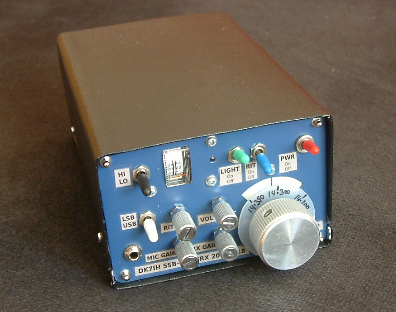
To give you an impression, that’s how the radio looks from the outside. Pretty “old school”, isn’t it?
The main design objectives were very simple:
- Compact in size (even without using SMD components),
- Analog VFO with vernier drive (1:10 gear) and variable capacitor,
- No digital stuff (=> no digital noise!),
- RF Output in the range from 15 to 20 watts pep in SSB,
- Single conversion superhet (9MHz interfrequency)
- No “save as many components as possible”-design.
First the block diagram giving you the basic structure of this radio::
“Old school” SSB transceiver for 14MHz by DK7IH (2018) – basic outline
The VFO
I decided to use an analog VFO in this project due to three reasons:
- It’s really old style,
- it is much less prone to produce any unwanted “birdies”, and
- phase noise performance usually is better than most of the digital ways to generate a signal.
For the VFO I chose the Hartley design characterized by a tapped coil. This type uses less critical components than a comparable Colpitts circuit thus reducing number of parts (2 caps in this case that are avoided) which might lead to unwanted frequency changes (drift).
How to build a VFO that is really stable
Lots of pages have been written about this topic. This another one. First, be aware of the fact that it is not possible to build a VFO that has the same frequency stability like a modern digital system. This is because these systems are all crystal controlled. But it is possible to achieve a drift of some dozen Hertz within an hour or so which is absolutely sufficient for having even a longer QSO.
The main problem is based on physics, or thermodynamics to say more exactly. All material expands when heated and contracts when ambient temperature decreases. OK, some exceptions exist, water below 4°C is the commonly known example of them.
Avoiding thermal runaway
Heat is the problem in such a circuit. It comes from the interior of the components when current flows through them and from the outside, for example when the transceiver is exposed to sunlight or placed near another source of thermal energy. Also heating of the final rf amplifier stages may contribute to heating the cabinet inside. The electronic parts forming the central strucure of the tuned circuit exert the main influence connected to thermal runaway of the frequency that is generated.
The general approach is: When we can’t avoid physical effects we must choose components that change their values in such a way to compensate the changing of the values of the other parts. That means we have to look carefully on temperature coefficients of the varoius components we intend to build into our VFO.
Choosing the “right” components for your VFO
Choosing advantageous components is crucial for frequency stability. So I did some brief research to find out more about temperature coefficients of coils of various types and available capacitors. Here are some of the outcomes.
Explanation of syntax: If a relation is negative, a minus sign (“-“) is given. In this case the value (C or L) decreases when temperaure increases. A plus sign (“+”) indicates a positive coefficient. When the relation of value change by temperature change is weak (that means no intense changing of the value when heated), there is only one “-“-sign. The more “-“-signs you have, the higher this respective ratio is. The same applies for “+”-signs to indicate a positive relation.
Capacitors:
- Ceramic capacitors: —
- Polystyrene capacitor: –
- NP0 (C0G) capacitor: no measurable effect
Inductors:
- Air coil on polystyrene coil former: +++
- Coil wound on T50-6 yellow toroid: +
Based on this short survey, the best combination would be NP0- and Polystyrene caps together with an inductor wound on an T50-6 (yellow) core. Hopefully their temperature behavoiur will compensate more or less and lead to best stability. Hint: On the photos appearing later in this text you will see an air coil wound on a TOKO style coil former that has been used because it does not need so much space.
The VFO circuit
I finally chose the Hartley circuit for my VFO. There it is:
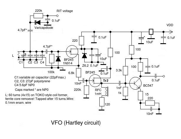
VFO Circuit explanation
Starting from the left you can see the tapped coil (here 60 turns tapped at 10 turns from the bottom end) on a 5.5 mm TOKO style coil former without any core. In parallel there are various capacitors (polystyrene and NP0 mixed) to build up the total capcity. It is common use to spread the total capacity needed to various single capacitors because it has turned out that the effects of temperature change are less significant if you use more (and therefore smaller) single capacitors.
A 100k resistor is used to pull the gate to ground and therefore provides a correct bias at the FET’s gate. The 1N914 diode is a so called “clamp” diode that has been installed to stabilize (and therefore reduce) the rf voltage in order to avoid excessive rf voltage coming to the FET’S gate which would lead to distortion. This diode has a negative side effect, but that an be accepeted for a VFO in the rf bands: It slightly increases phase noise because it works as a regulator. With some the designs you can see this diode in reverse position, don’t worry, the regulating effect takes place either.
To ensure the oscillator to produce radio waves, in-phase feedback between gate and source is generated via the tap you can see with the coil. A tap of about 1/6 of the whole number of windings provides enough feedback voltage to let the oscillator start by its inherent thermal noise and generate clear sine waves afterwards. Putting the tap too close to the “hot end” will cause distortion because the amount of energy coupled back to the gate will be too high. Also instabilites are probable because of excessive drive power to the gate of the FET.
On top of the tuned circuit there is a varactor diode that is used to be controlled by a positive voltage to form a RIT (receiver independend tuning) control circuit. It is very loosely coupled to the tuned circuit to minimze temperature effects and because only 1 or 2 kHz “swing” is needed. The generation of the RIT voltage will be described later in this text.
The main tuning capacitor
An air capacitor is mandatory here! You can either use a ready made one from the surplus market. But to keep it as small as possible I built my own by dismanteling one of old variable capacitors formerly used for homemade AM radios. Use a small drill to remove the rivets, dismantle the capacitor completely and rebuild it again as an air capacitor (get rid of the plastic dielectric interlayers!) by using M2-screws and nuts. Youl will have evenings of endless fun with this game! 😉
Buffering and amplifying the Signal
The second stage with another FET is very loosely coupled to the source of the first FET. This is made to minimize effects of load changes to the frequency. This stage is a so called “source follower” giving a very low impedance signal to the final stage that is responsible for the amplification of the signal to a level of 2 to 3 volts pp which you will need for the rx mixer that has been designed as a dual-gate-MOSFET mixer (see receiver chapter later!).
DC voltage in the VFO
Voltage stabilization is crucial for best performance of this critical part of the radio. Supply voltage changes always lead to frequency changes. So a two-level buffering is common use here. The first (and most critical) stage is buffered twice (10V voltage regulator integrated circuit 78L10 and subsequently by a 6.2V zener diode) whereas the buffer and the amplifier stages are supplied with 10V regulated DC voltage only.
Ambient thermal isolation
To avoid the VFO being affected by interior thermal convection (flow of warm air inside the cabinet) it is recommended to shield the VFO from the rest of the transceiver. I do not recommend using metal sheets as walls here because these form other unwanted capacities that will lead to thermal effects on the generated frequency. Metal also is a good conductor for thermal energy, so you might run counter to your goals. My thermal insulation therefore is made of simple cardboard.
The Local Oscillator (LO)
This oscillator is much more uncritical than the VFO because it is crystal controlled. The purpose of the LO is to supply a carrier signal for the SSB modulator. Due to the fact that there are two sidebands we theoretically can use this LO must be switched to either one of two possible frequencies. In case of an interfrequency of 9MHz (9000kHz) these are: 9001.5 kHz for the first sideband and 8998.5 kHz for the second sideband. Please note that I did not write “USB” or “LSB” because the frequencies forming each sideband might be changed because of the frequency plan of the transceiver where by mixing with the VFO frequency the sideband might be inverted depending on if you add or substract the VFO frequency from the 9MHz-SSB signal.
There are several possibilities to produce these two frequencies:
- Using two different oscillators each equipped with a single crystal,
- switching two crystals with one osillator,
- using a variabale capacitor or a coil to “pull” one crystal to the desiered frequency.
Discussion:
- This method means high effort but surely is the most exact one because there are no influences of the unneeded choice to the other crystal currently on duty.
- Is the worst idea because the unswitched crystal is highly prone to influence the freqeuncy of the switched one because they are linked to parasetic capacities within the wiring, the switch and so on. Forget this one espacially when using the internal oscillator of a NE602/SA612!
- This to my point of view is the best compromise between circuit simplicity and function. You can see this way of sideband switching in my transceiver.
This is my local oscillator:
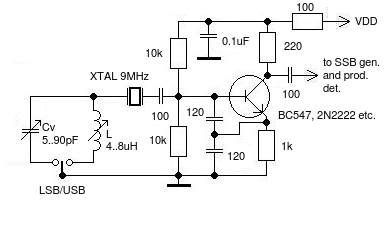
It is a simple Colpitts circuit where in-phase feedback and feedback voltage control are achieved by a series of two identical capacitors. A simple switch, a capacitor (90pF max.) and a coil (4 to 8uH max.) that are either connected to the base of the transistor via the 9MHz crystal determine the sidband freqeuncy of the oscillator. Signal is taken out via the collector.
The Receiver
The receiver will be presented step-by-step starting with the front end stage:
The RF Preamp
This stage is connected to the antenna relay. It provides an amount of basic amplification for the antenna signals. But that is not the main purpose. Noise figure improves significantly if you use a stage with low inherent noise. Thus a dual-.gate MOSFET is installed here. This semiconductor is also used to control stage gain because gate 2 of the MOSFET is connected to the AGC chain of the transceiver. About 12 dB gain swing are possible here. Stage gain is about 15dB.
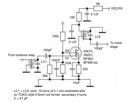
Note the position of the primary and secondary windings of the input and the output coil. To avoid self-oscillation the output (drain) of the MOSFET is connected to the untuned part of the LC circuit. Coils must be shielded and should be equipped with ferrite heads (in the photo the piece in left bottom corner).
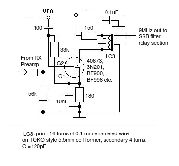
The Receiver’s Mixer
In this stage also a dual-gate MOSFET is used. This type of mixers provides good capabilities to cope with high signal levels without producing unwanted signals (high IMD3), gives some dB of gain and is low-noise also.
One “disadvantage”, if you want to say so, is that it needs a little bit of higher VFO drive (about 2 to 3 volts pp). Gate 2 bias is generated via the voltage drop on the source line. The tuned circuit in drain line is adjusted to the desired interfrequency. See the schematic for the exact winding data and parallel capacitor.
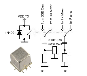
The SSB Filter section
Transmitter and receiver share the same SSB filter in this transceiver. So some sort of switching is recommended even if circuits exist that go without one. I used a high quality relay made by Teledyne that I bought in a 10-piece bundle for low price (1€ each!) via a well-known internet marketplace. Caution: Some SMD-relay I tested prior to building this rig were disastrous concerning signal isolation between terminals. To avoid any disappointment or frustration I recommend testing a relay before you finally install it.
All connections to the rest of the circuit must be made with shielded cable. I found an interesting alternative: I sometimes design my own very thin shielded “cable” with brass tubing (1 mm inside diameter) where I put insulated cable inside. The brass tube is connected to GND on the Veroboard. You can not bend these tubes but longer lines can be interrupted for a short piece so that the “bend” can be made by putting two parts of tubing in 90° degree angle for example.
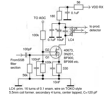
The IF Amplifier
This one might look familiar to you. It is a simple “remake” of the front-end stage. The one remarkable thing is the secondary of the output transformer. This coil has 4 windings (prim. 16 turns). The secondary is center tapped (2 + 2 turns). This is because the product detector (SSB demodulator) has a symmetric input. Very important in this stage is the 100uF capacitor in VDD line. This cap prevents the stage from AF resonating and self-oscillations on the VDD line and makes the receiver much more “quiet”.
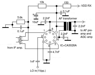
The SSB demodulator
This stage is probably the most “old-school” part of the whole transceiver. It uses an old CA3028A differential amplifier as mixer circuit:
You won’t be able to buy large amounts of this IC anymore. And if you get one, the prices are close to or beyond a rip-off. But there is an alternative. You can build your own “IC”. Watch this page where all the information you need is provided!
Signal input goes to the paired transistors forming the amplifier stages. LO is fed into the line transistor that is used to set the current of the differential amplifier thus providing a switching and therefore superposition of the two signals.
The output circuit is made of an audio transformer formerly used in the final audio amp of old AM radios (coil resistance is about 300Ω each side). The 2.2nF capacitors eliminate remainders of the rf signals and “ground” the terminals of the AF transformer.
Audio amplifier
This final receiver part consists of two stages: An audio preamplifier with a bipolar transistor and a final amp with a TBA820M integrated circuit.
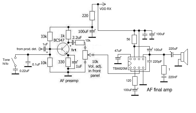
The two caps 0.22 and 0.1uF determine how the higher frequency components in the audio signal are cut off. The higher the total value the more the higher frequency components of the audio signal will be limited due to the equation XC=1/(2*PI*f*C).
Tr1, which is a universal purpose NPN transistor, provides high gain. Thus a 10k resistor is installed to form a voltage divider with the audio gain potentiometer.
In the final stage I use a TBA820M ic (8-pin DIL version). This one is more linear than the well-known LM386 that you usually can find in this place and it is not so prone to self-oscillation. The cap aside the 100uF in the top left corner of the schematic is not marked, its value is 0.1uF.
Loudspeaker impedance is 8Ω.
The AGC
Automatic gain control makes listening to signals much more comfortable. AGC voltage is audio derived, like in my other transceivers. The circuit also is nearly the same:
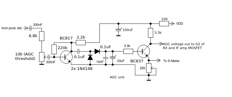
Due to the very high gain of the product detector this stage is directly connected to this circuit and not to the AF preamp. A potentiometer is used to set the threshold of the AGC onset.
Next stage is a simple audio preamplifier followed by a “Greinacher Circuit” serving as voltage doubler and providing DC voltage proportional to the audio signal level. A dc amplifier with another NPN transistor lets its collector voltage drop as soon as it is fed with significant dc input voltage. Thus this voltage decreases and so it can be used to control gate 2 of the MOSFETs in the various receiver stages that are equipped with tetrodes.
The S-Meter is connected to the emmitter of the final transistor. If conductivity in the transistor rises, the emmitter becomes more positive and the S-Meter needle is deflected proportionally. The 220Ω potentiometer in the emmitter line must be set in accordance to the respective S-Meter you are using. One shortcoming should be mentioned: If you have a not so sensitive meter then the value of the pot can be set to nearly 100Ω or above. This will prevent the collector from dropping to nearly 0V in case there is a strong signal and hence reduce the maximum dB you can get from the AGC chain.
The Transmitter
The transmitter section is designed for an output level of about 20 watts and uses 4 stages all equipped with bipolar transistors. The last stage is a push-pull stage, the 3 low-power stages are single ended. I prefer push-pull for the last stage (if possible) because this circuit inherently does not create even harmonics thus simplifying output filtering.
The first parts of the transmitter to be shown here are the microphone amplifier, the SSB-generator and the TX mixer:
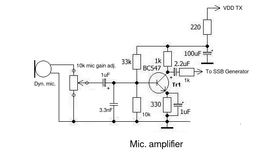
The mic amp is simple but provides enough gain and good linearity for using an old-style dynamic microphone. It works in common emmitter mode and has gain of about 15 to 20 dB.
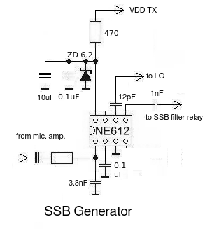
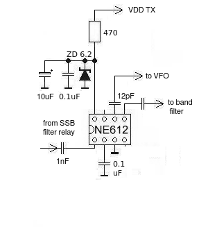
The audio signal amplified by the microphone amplifier is fed into PIN1 (Input 1) of an NE602/SA612 mixer IC which is the simpliest way to generate a DSB signal with a Gilbert cell. LO input is fed to PIN7 and should be in the range of 200 to 300mVpp. Thus a 12pF cap has been installed to limit LO voltage going to input at PIN7.
Carrier suppression is around 45dB when LO offset frequency is correctly set for each of the two sidebands and LO voltage is not much higher than the 300mVpp mentioned before.
The DSB signal produced by this mixer goes on to the SSB filter relay and filter that has been described before. The use of shielded cable is mandatory, too.
The TX Mixer
You won’t be able to recognize many differences if you compare this TX mixer to the DSB generator. In fact, there are none.
The 14MHz Band Pass Filter
Next is the band pass filter that consists of 2 coupled tuned LC circuits for 14MHz. They are also wound on TOKO style coil formers. Data can be found in the schematic underneath.
It is important to also install the ferrite heads that are provided with most of the coil formers and to use the shield “metal cans” that are also standard for these coils. This is to prevent stray coupling of rf energy into the first stage of the power amplifier strip and therefore preventing self-oscillation of the transmitter strip.
For proper adjustment set the transmit frequency to about half of the frequency swing ((i. e. to about 14.200 kHz) and tune for max. output.
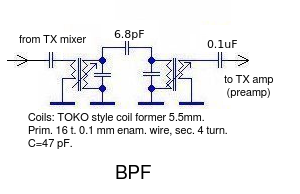
If you modulate with a two-tone signal to the mic amp you should see about 500mVpp by the output of the BPF when the chain is fully driven.
The Preamplifier
We start with the low power end of the power transmitter section. A bipolar rf type transistor is the center part of this stage.
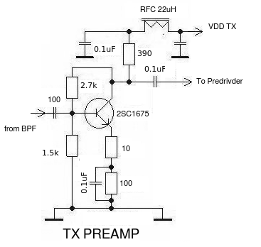
This one is a standard circuit and has been “trimmed” for maximum linearity in order to reduce distortion to a minimum (which is also true for the following stages). You can see the well understood 2 master ways of achieving max. linearity in an amplifier stage:
- Negative feedback between collector and base (i)
- Emmitter degeneration (II)
Explanation:
i) The first measure goes along with the 2.7kΩ resistor between collector and base of the transistor. This resistor provides positive dc bias voltage to the base and leads 90° out-of-phase ac voltage to the transistor’s input. This reduces gain and therefore distortion. But due to the fact that the whole transmitter strip has plenty of gain, this loss in gain is not a serious problem.
ii) The 10Ω resistor in the emmitter line is not bypassed by a capacitor. This stabilizes the circuit. When the current through transistor increases the emmitter voltage will rise (according to Ohm’s law) and the voltage between collector and emmitter drops. This reduces voltage difference between base and emmitter and hence also reduces gain.
The coupling to the next stage is done by a capacitor of 0.1uF. This causes some impedance mismatch. But that is as well not a big problem because the gain reduction here helps to prevent the whole transmitter from unwanted oscillations by diminishing overall gain.
The Predriver
This stage is somehow a copy of the stage before but allows more current to flow through the stage. It is also operated in class “A” mode and uses the same methods to maximize linearity like the preamp stage.
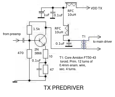
You can use a 2N3866 transistor here which is available. But any other rf power transistor for driver stages (2SC1973 etc.) will also do the job well. A heatsink is recommended even if stage current ist not that high. T1 should be a toroid, a “pig-nose” core in this place to my experience is not the best choice. The 10uH RFCs are ready made ones but you can also wind 20 turns of 0.4mm enameled wire to a FT37-43 toroid core.
RF output of this stage could be measured as 100mW into a 50Ω load.
The Main Driver
This stage has an old 2SC2078 CB transistor and is operated in class “AB” mode. An alternative could be a 2N3553 that is available on ebay for example. A heatsink is neccessary for whatever type you use.
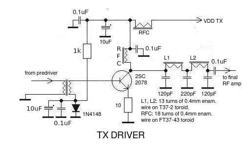
Correctly set bias for “AB” operation is ensured by the 1kΩ resistor from VDD to the bias circuit. The 1kΩ resistor limits the current whereas the diode works as a stabilizing element (thermistor). It must be connected directly to the case of the transistor ensuring good thermal contact. If the temperature of the devices rises the resistance of the diode will decrease. Hence current through the diode increases thus reducing the part of the current that can pass through the base-emmiter line of the 2SC2078. Quiescent current is stabilized and thermal runaway is prevented.
The rf output is uncommonly terminated with a low-pass-filter. This is because I first intended to build the transceiver for an output level of about 4 watts. But then I had the idea that the space still available on the veroboard could be used by another amplifier definitely leaving the QRP power level. So I left the circuit how it first was and just added the final amplifier stage.
Output of this driver stage now ist set to 1 watt into a 50Ω resistor.
The Final RF Amplifier
Now let’s go for the power machine in this transceiver:
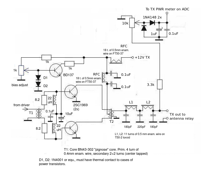
2 rf power transistors 2SC1969 by Eleflow provide up to 20 watts of rf power. Bias for such a high power stage can not be set by a simple resistor. Here a line transistor (BD137) serves as current control. Diodes D1 and D2 (1N4002 or equ.) follow the same purpose like the single one in the stage described before. They must be mounted with excellent thermal contact to each of the 2 power devices which ensures secured protection against thermal runaway. The transistors also must be connected to a large heatsink. I use Aluminium metal strips (2mm thickness) to connect them to the back wall of the cabinet.
RF is fed into the power transistors via a network of 8.2Ω resistors and two 22uH rf chokes that seperate the rf line from the dc bias line letting only dc pass. This method makes construction of the input transformer easier. Winding ratio is 4 turns primary, 2 turns secondary. This is because the input impedance of the stage ist fairly low (aorund some ohms).
The output transformer is a homemade “pig-nose” of 6 toroids FT50-43, where 3 toroids are stacked (using 2-component glue) and 2 of these stacks are glued in parallel (see picture at the end of this text for details!). Winding ratio is 1 + 1 (primary center tapped) to 4 on secondary.
Quiescent current of this stage should be set to about 100mA.
A low-pass-filter terminates this stage and is connected to the antenna relay.
In addition you find a section to measure rf power. This is again the so called “Greinacher-Circuit” which doubles the voltage and serves as a charge pump. The dc output of this circuit directly leads to the S-Meter indicating output power of the transmitter.
Performance
First the spectrum of the signal with the transmitter fully driven to 20 watts output power with a two-tone-signal:
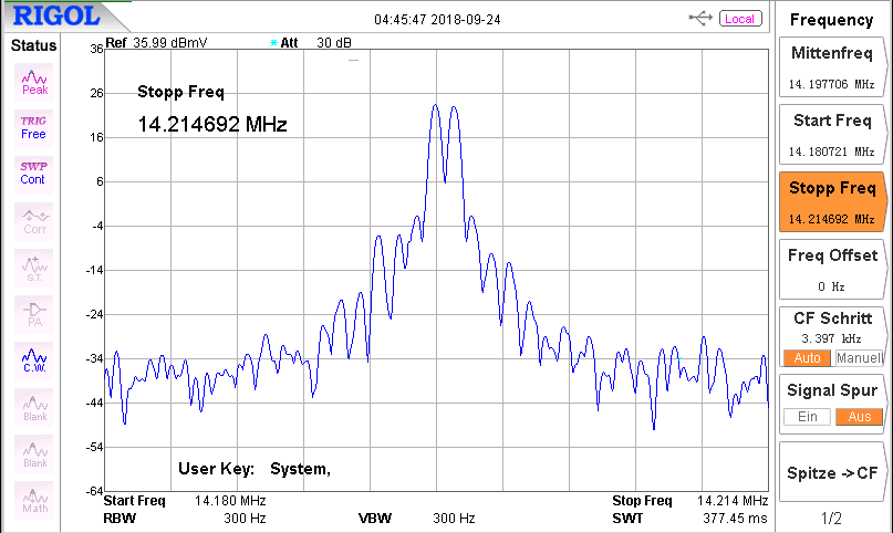
IMD3 is about 28dB below signal peak which I think is acceptable.
Amplitude diagram is as follows:
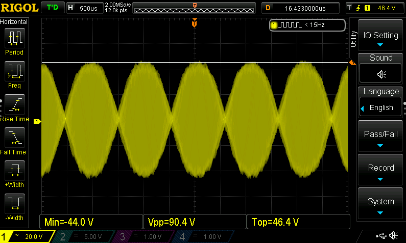
Max. radio frequency voltage is 90.4Vpp which calculates to about 20 watts of rf power (P=(Vpp/(2*SQR(2)))²/50Ω).
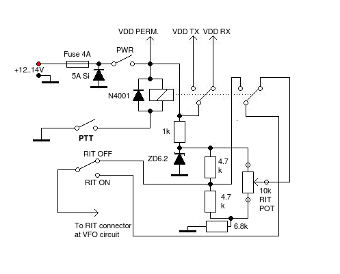
Power switch board and RIT voltage
A 12V relay with two pairs of contact sets is the heart of this unit. DC power is lead to TX, RX and permanent supply via the respective power lines.
RIT voltage generation is a little bit more complicated. When the RIT switch is in “OFF” position, RIT voltage always is taken from the fixed voltage divider that is formed of the two 4.7k resistors either when on receive or transmit mode.
If RIT is “ON” then there are two possibilities: When on receive mode, RIT voltage is gained from the 10k lin. potentiometer in the front panel. When on transmit mode RIT again is taken from the fixed voltage divider.
There is also a false polarity protection diode. This can be any silicon type with max. current >= 5 A.
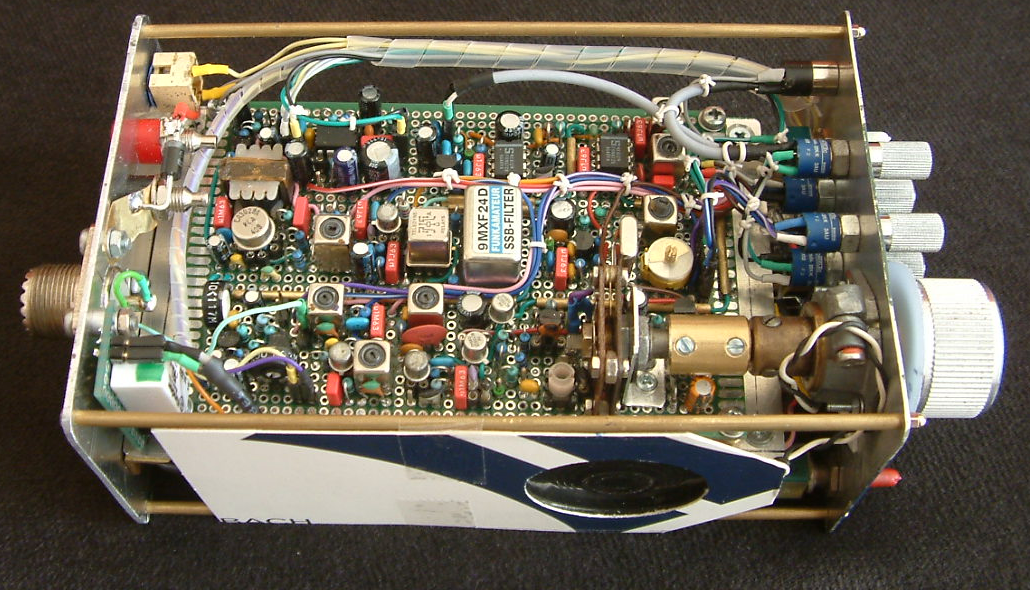
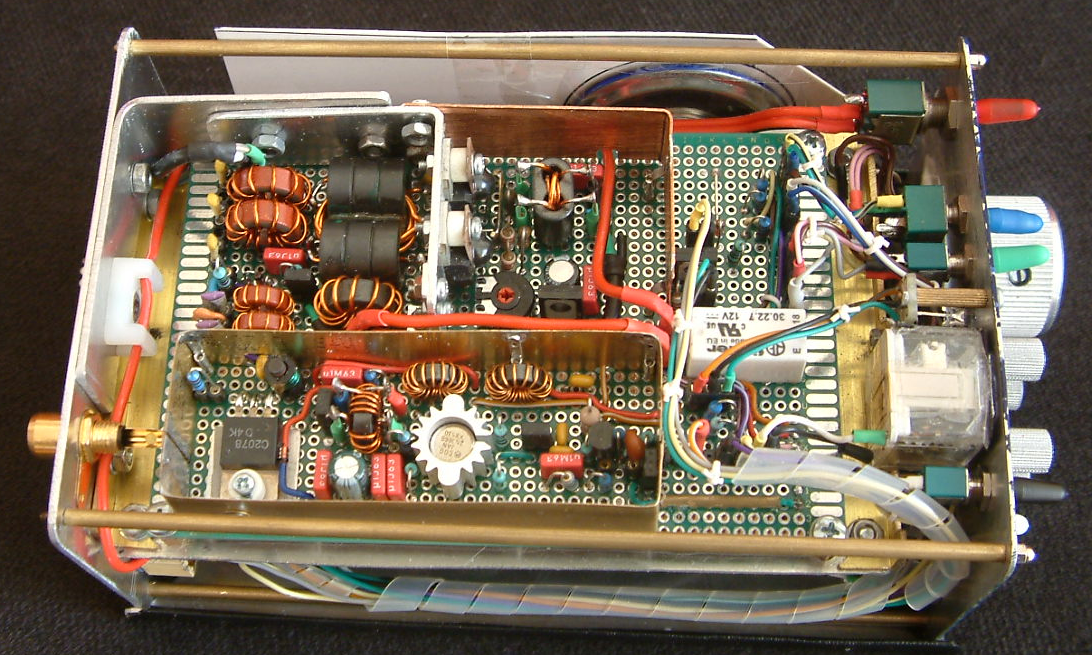
Mechanics
The construction is sandwich style made of 2 layers:
OK, that’s the story. Thanks for joining me on the trip to the past! 😉
73 de Peter.
I’m absolutely amazed at the construction of your rigs (and at how many you have built over the years!) I’ve collected quite a collection of old parts myself (I bought out the last of Jameco’s CA3028A’s some years back when they were having a ‘fire sale’ on them). Now I’m designing a home brew 20 meter rig using some of your ideas.
I will use a ca3028 in the RX mixer and IF amplifier, MC1496 in the bal mod, 40673 or mfe301 rx rf, ne602 prod det & tx mix. Lm386 af out. Xtal filter at 10.7mhz was removed from an old CB radio. Will use your idea of si5351a as vfo/bfo switching output frequency between rx and tx as mixers change role. Final will be MRF476’s, 2n3866 driver. I guess I could follow your tx chain you have here using MRF476 as driver and MRF475’s in final for 20-25w out. This mono bander will be a test bed built in a small 6″x6″x2.5″ surplus mini box.
But I also have plans for a multi bander in an old amo box (to take to field day).
Hi there scharkalvin,
good ideas, maybe you can report when you have finished the rig or at least parts of it.
BTW: Using a 10.7 MHz IF is not recommended when building a 14MHz rig with an analog VFO. Then the VFO frequency has to be in the range of 3300kHz to 3650kHz. This will end up in a problem when you tune to to 14.266 MHz. Then you will receive the third harmonic of the VFO now oscillating on 3566kHz.
I had that problem 30 years ago when I stripped also a 10.695 MHz SSB filter from an old CB transceiver. A system of 2 equations brought me to the point after the problem had been recognized:
fRx – fIf = fVFO (I)
fVFO * 4 = fRx (II)
After having solved these equations I was a little bit more experienced. 😉 But then a Si5351 was not invented yet. So nowadays I would just put the VFO frequency above the IF and then the problem is solved.
73 de Peter
That’s why I’m planing on using the si5351. I also have an 11.2mhz filter from another CB rig as well as some 400 pcs of 8338mhz crystals that could be used to make filters. I’ve already written the Arduino code to run the si5351 with a 32×128 OLED display, including mode switching for USB, LSB, CW, sig gen mode, and calibrate mode (to compensate for off freq crystal). When I’ve done some more testing I’ll put the code on github and post a link to it.
Another fab build. I am amazed that your compact rigs don’t howl with RF feedback, so much power in such a small space, and you don’t have the benefit of large PCB ground areas. Well done! –VK3HN.
Hi Paul, the grounding is not a severe problem. I use self-adhesive copper foil for grounding plus small brass sheets on component side as shields that are connected to GND. Plus there is an aluminium frame aorund the whole board also connected to the GND conductor of the circuit in several places.
In my larger projects I divide the circuit into small units (modules) that are placed on single veroboards. Each corner of these boards has a conductive plate connecting a brass washer to the sheet metal carrying the boards. If there is space I additionally place aluminium sheet metal vertically between the modules. I am currently working on a high performance 100W transceiver for 20m which I‘m going to introduce in one or two months. There this technique will be explained. 73 de Peter
I’ve been having some bad luck with my build of a 20 meter QRP rig inspired by your ideas. RF stage using an MFE300 dgmosfet with double tuned input bpf and a single tuned output link coupled to CA3028 mixer. The RF stage easily breaks into oscillation. Have a shield between g1-g2 and s-d. As I try to peak the input driven by grid dipper and watching the output on a scope, I can see the signal doesn’t quit as I back off the drive. Lower the rf gain (g2 voltage) and oscillation quits.
I’m thinking I’ll rip out the tuned circuit in the drain and replace with a broad band trifilar wound FT50-43 to drive the ca3028 instead of the bifilar link on the tuned circuit on T50-6. At least I know that the old DGMOSFET is working!
Already debugged the MC1350 IF stage (it was also oscillating, but with untuned input capacitor coupled to xtal filter). I put a 5k resistor across the output tuned circuit to tame it.
The Si5351 vfo/bfo is working. Rewrote the software to provide output 0 as bfo-vfo for prod det/tx mixer (NE602), output 1 for vfo to rx mixer (ca3028), and output 2 as co to bal mod (mc1496).
Yes, it is not recommended to have a tuned circuit on the gate and the drain side the same time with a dg mosfet. I then put the untuned part of the LC device to the gate because I have the tuned part of the input bpf to the gate because of the better impedance matching. Replacing the output transformer with a broadband one cost you some gain but it is a good solution. Even when taking into account that selectivity fo your front end might lack a little bit.
vy 73 de Peter
Over recent weeks I have built 3 dual gate mosfet amp stages, one as an 80 to 20m RF stage, and 2 as IF stages, to be used each side of the crystal filter. I have also built your AGC stage. Starting with your component values, I used no tuned circuits at either input or output, and got stable but underpowered amplifiers, maybe 6 to 8dB gain. I then replaced drain resistors with 8T bifilar on FT37-43, resulting in higher gain, around 12 to 15dB. Again perfectly stable. As the mixers are gainy SA612s (not lossy DBMs) I’m going to leave all three stages as they are. Initial receiver testing suggests that overall receiver gain is about right, with the AGC range as you describe.
One comment, the DGMosfet sources are not lifted above ground with an LED as per other designs, meaning the AGC doesn’t completely cut off these gain stages. But in another receiver, this mechanism has caused the AGC adjustment to be fiddly, and to pop the audio as stages close and open.
Thanks again for your excellent designs. Paul VK3HN.
Hi Paul, I did not use the LED circuit due to reasons I can not explain. 😉 But the result that you said is correct: You reduce “gain swing” to a certain degree. But it is a good idea to try that with the next receiver I’m gonna build. A blue glowing radio inside. 😉
By the way: Recently I visited your website and found excellent work. I commented to one of your articles but my comment was rejected, maybe because my WP account was not accepted in spite the fact that I was correctly logged in here as “DK7IH”. Strange. 😉
73 de Peter.
Oh, sorry, your comment from Dec 13th was sitting in my WordPress spam queue. Unusual, I never look in there because it is always only genuine tasty spam. Thanks for your comment! Now approved. WordPress should auto accept your comments now.
I am building your dual symmetrical SA612 transceiver, with relays to switch the mixers around. Receiver is working FB. Blog post and video soon, another month’s hobby time needed to completion. I have a weekend in the south east Australian alpine region booked for early February 2019. Aiming to activate some summits with the new ‘compact’ rig there! 73 Paul VK3HN.
Excellent idea and buildup
I liked very much.
73
VU2TRF
Thank you! 🙂