FYI: 4 and 1/2 years after having published this article I have built another multiband HF radio with some new features and an improved design:
An experimental HF 6-Band SSB Transceiver
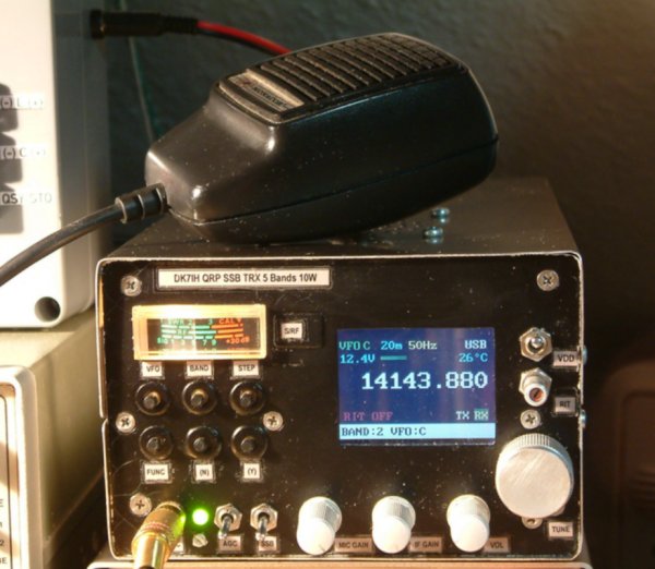
I owned an old ATLAS 215 RF transceiver once. This unit was destroyed because by a momentary laps of reason. I put 12 V DC to it with wrong polarity. Sh..! Since this very sad day I’ve always wanted a new 5 bander rig. OK, I could have bought one. Money is not the big problem. But, as a passionate homebrewer, I thought to myself: “Why not building a 5 band trx instead of the monoband rigs that I’ve built so far?“. This decision was made in summer 2015. Now, in late autoumn, this rig s nearly completely finished.
So, let’s tell the whole story…
General aspects
Building a multi band rig is, as you might conceive, much more complicated than setting up a monobander. Seems sensible. So, first I went through literature to avoid fulminant project failure which is more probable when making serious mistakes that can easily be avoided by careful planning.
What to read? First, “Solid state design for the radio amateur” by Hayward and DeMaw is still a very useful book. Even when sometimes people mail me and say “Oh boy, why are you always bulding all those nostalgia radios with old style components like the ‘741’? Boy, today, SDR is the standard!“. My simple answer then is: “No, it is NOT!“.
To learn more about multi band QRP transceivers I also browsed the web for similar projects. There are some, but often there is no full cicuitry given. Here are two sites that might be interesting: M0DGQ and VK3EPW.
So, after some days of conceiving, I finally had the basic concept in mind. Mixing the modern times (DDS and microcontrollers) with the old style of QRP homebrewing. And what about “SDR”? Sorry, not on the agenda. Based on these prerequisites, here are the main ideas for this radio:
- DDS controlled by microcontroller
- Colored graphic LCD
- 5 ham bands (80, 40, 20, 15 and 10 meters) to be covered
- SSB only
- 10 Watts out, transmitter equipped with bipolar transistors in push-pull mode (lots of CB-types still on my stock or replaced e. g. by ELEFLOW types)
- Single conversion superhet receiver with AGC and high dynamic range (diode ring mixer). Must be able to deal with high signal levels on the lower ham bands.
- Compact size to make the radio fit for portable, outdoor and holiday use (flight!)
- Using “The usual suspects” like NE602, MC1496, LM386, MC1350 to be involved.
To avoid any fuss in recevier and ssb generation design I have again picked up the single-conversion principle that has successfully been applied in my former transceivers which uses only one interfrequency (IF). One of the reasons for this, besides circuit simplicity, is the fact, that a single conversion superhet produces less “birdies” than a double conversion one. Birdies are a particular problem when you use DDS frequency generation. Every DDS produces spurii that can be received with more or less intense signal strength in your own receiver. So I was not keen on having more than the inevitable number of self-reception signals by adding a second interfrequency.
Mechanical considerations
I love to build rigs that are compact and neat. I don’t like the bulky boxes only capable for home use. To make this fairly complex radio not too large, I found that sandwich design would be the best way to save space and make the transceiver friendly for building and service.
Based on the “sandwich-idea”, the rig consists of three different layers:
- Transmitter board
- Switch board with final low pass filters (centered between the two others)
- Receiver board
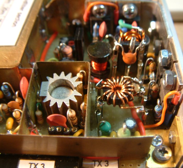
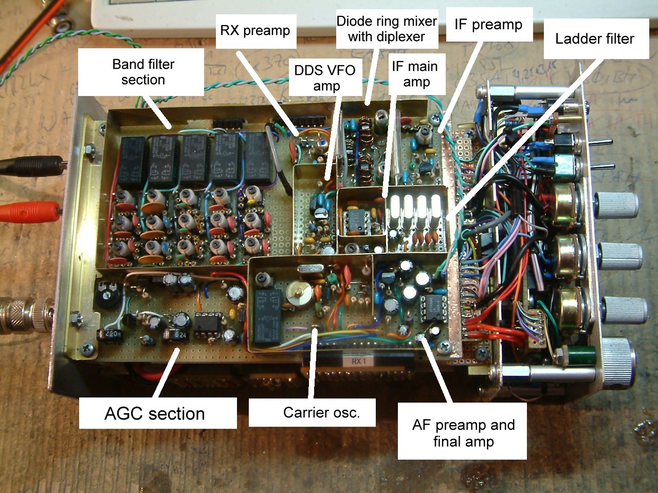
All boards are connected from the laterals by a homemade plug system so that the single Verobaords can be removed and reinstalled into and from the assembly quickly. Here’s an overview picture showing this construction method:
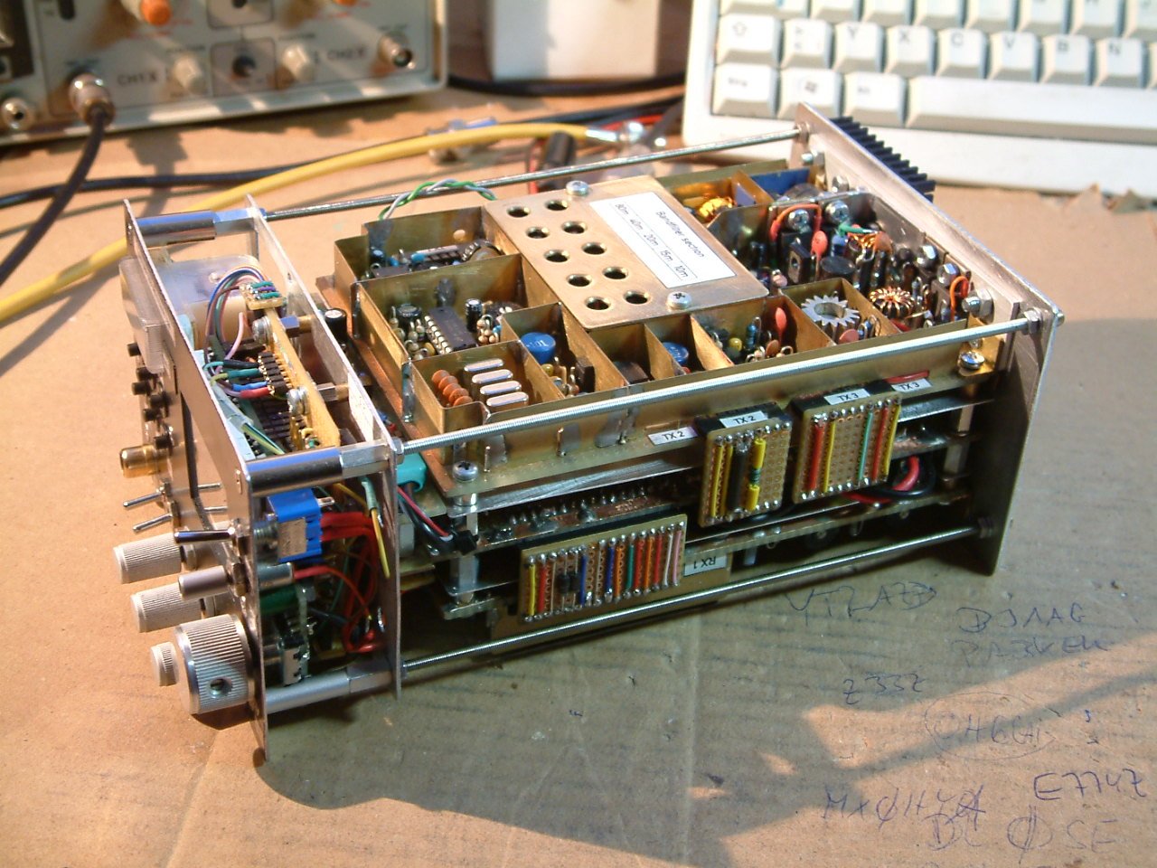
In the middle of the sandwich you can recognize the switching unit from where the plugs are lead to the receiver and transmitter board. The idea behind this on one hand makes the transceiver very compact. On the other hand it is very service friendly. It takes only 1 or 2 minutes for example getting the transmitter board out for changing a component. Pull the side connectors, remove 4 board screws + 3 screws at the rear-mounted heat sink and take out the board. Remounting the board takes some seconds more. But there is no need to disconnect and reconnect an endless number of cables each time you perform a modification. All lines are connected by the side-plugs. And that’s it! One shortcoming should be mentioned: When I built the rig there was a little bit more effort concerning wiring. But it pays!
As board No. 4 the DDS-VFO together with the microcontroller and the LCD have been put behind the front panel.
VFO and LO frequency considerations
In this transceiver the interfrequency (IF) is 10 MHz which is based on the fact that respective crystals can cheaply be purchased in larger quantities to build appropriate ladder filters with. I bought about 50 pieces for around 10 Euros. But other crystal frequencies are also possible. For example computer crystals of 9,832 kHz, standard 9,000 kHz xtals or others in the same frequency region can be used. Taking your IF between 8 and 12 MHz might be the best choice in my opinion.
Hint: Before choosing the final IF and purchasing crytals or ready-made filters it is highly recommended to do some basic calculations to ensure that none of the harmonics either of the VFO or the LO falls into the desired receiving band going together with a certain set of frequencies generated by the two oscillators.
So watch out where the frequencies of VFO and LO are located in the radio frequency spectrum! A spreadsheet software is extremely useful for this purpose, because you can change the IF quickly and see at first glance what you will get out when the DDS is about to generate the needed frequency to bring you to the desired band. Also keep harmonics in mind!
And also keep in mind that the image frequency on every band should not fall into shortwave broadcast bands (e. g. the 49m-band!) where strong off-the-shelf stations may appear. OK, sometimes this can’t be avoided but it’s worth thinking of it before you start to build.
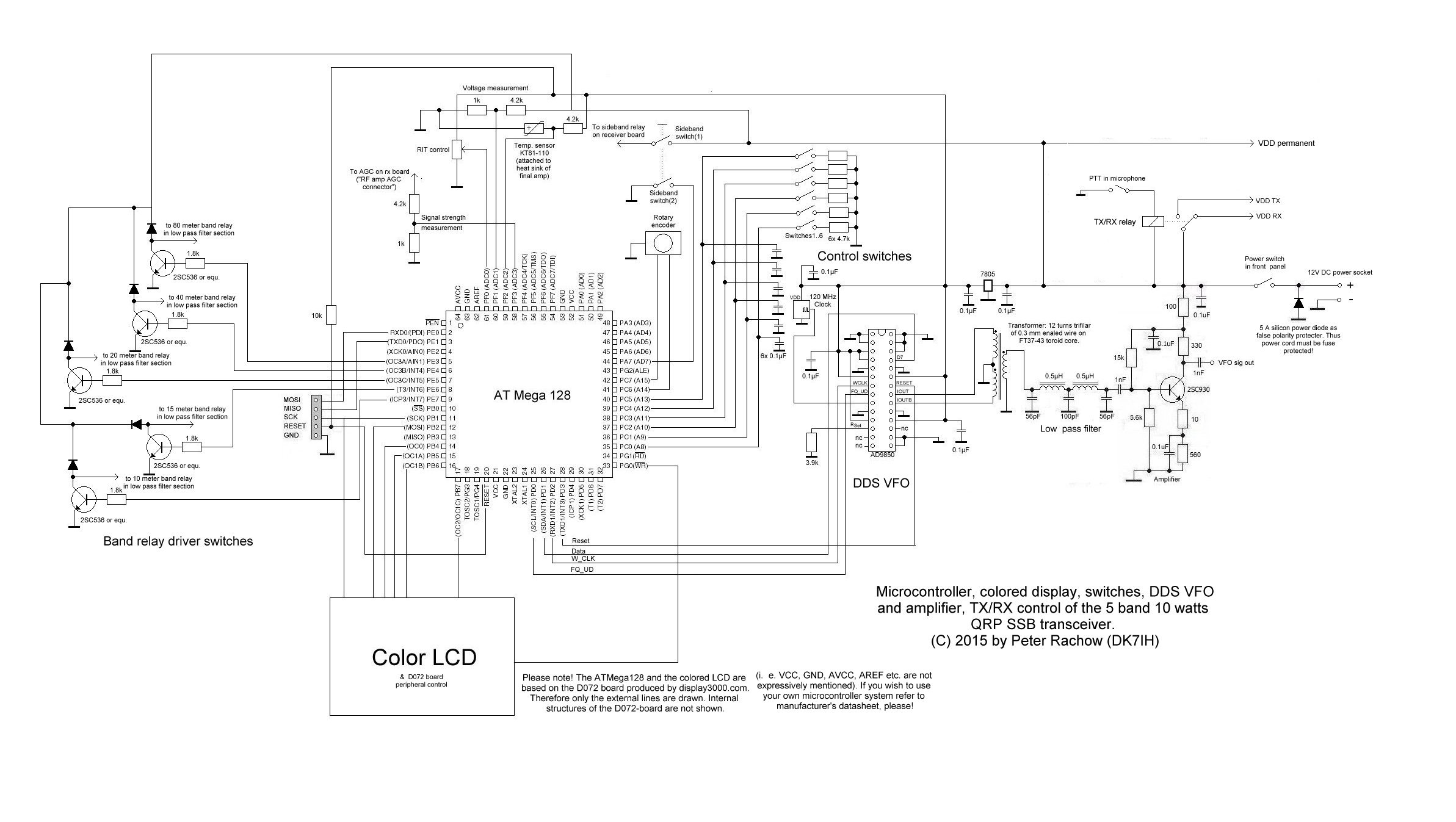
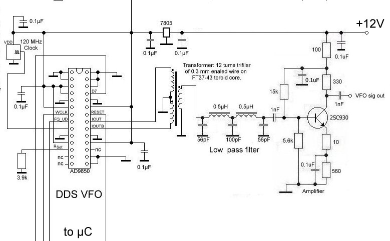
As said before, my rig uses a DDS system for obtaining versatile VFO functionality (equipped with an AD9850 made by Analog Devices). To get “a feeling” for this chip I first used one of those AD9850 modules available from China on ebay for e few bucks. The problem: They are more or less crap. at least for RF use. I don’t know what chips they install there, but the board was cheaper than buying a single AD9850 on the free market. No more questions. These boards produce a large number of spurii (aka “birdies”). A much greater number than I ever encountered with my last rigs using an AD9835 DDS chip that is nearly spurii-free. So I decided to buy some surplus original AD9850 chips and a breakout board to which I soldered the DDS chip and tried my own DDS board. It worked from the start. But there are also some spurii so I changed the AD9850 DDS to an AD9834 which is similar to the AD9835 from my other rigs. The AD9834 can be overclocked to about 100 MHz which makes him a candidate to substitude the AD9850 in the DDS. In the end I decided to use a more professional DDS by Analog Devices and came to the AD9951 that is also used in Kenwood’s TS590 transceiver. This one, as you might gues, worked best. Here is the description of this optimized DDS vfo.
Realizing the Transceiver
The DDS-VFO, the microcontroller and the colored LCD
Please note that the AD9850-based DDS has been replaced by an AD9951-system. Read the article here!
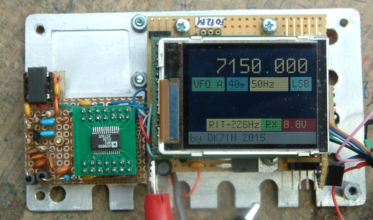
For a long time I have owned some colored LCD cellphone displays from a dive computer project that I had completed some years before. These boards are equipped with an ATMega128 micorocontroller which is capable to deliver enough capacity and calculation power even for extended software. So why not using this surplus material?
First, here’s the scheme of this unit:
Here’s an older picture of the practical realization of this DDS-VFO (running an older version of the software) with the LCD built in behind the front panel of my transceiver:
Why is using a DDS really cool?
What always was a problem in “pre-DDS”-times was to switch the VFO to the desired band. With the old 80/20-meter transceiver concept this was not a big problem, the 5-MHz-VFO did the job on either band. But it things were more complicated when you wanted to cover the other ham bands with only one VFO. Some basic concepts were switiching the coils and/or capacitors or bulding a superheterodyne VFO that mixed a basic VFO signal to the desired frequency. Lots of birdies included, sometimes at least.
With an appropriate DDS no superheterodyne or LC-switching circuitry is required to get the wanted VFO signal for each band. The AD9850 is capable of being clocked with 125 MHz maximum rate. The AD9951 can be clocked to 500 MHz even if 400MHz are nominal by the manufacturer. Due to physical reasons (Nyquist frequency) the highest frequency you can get out of such a DDS is about one third of the clock oscillator frequency what in the first case means about 40 MHz. So you can easily recognize that you can get all the VFO sigs from the one DDS you need to drive an rf transceiver without that VFO fuss well known in the older times. In my rig I achieved to stay very much below the margin of 40 MHz because output voltage due to the frequency calaculation you can see underneath. Keep in mind: Signal quality of the DDS decreases significantly the closer you get to its maximum frequency. Among other reasons this is due to the fact that a low-pass filter is switched to the output of the DDS. I recommend to stay at least 5 to 10 times lower than Nyquist freqeuncy if possible.
Frequency calculations
For the two lower bands (80 and 40 meters) the operating frequency is calculated by the following scheme:
f = fif – fVFO (I)
For the upper three bands (20, 15 and 10 meters) another equation is used:
f = fif + fVFO (II)
Two effects are desired by using this scheme:
First, there is no requirement to switch the local oscillator because it is always on the “right” sideband. The sideband relay in my rig is without current except from those times when you want to use the “wrong” sideband. Second, the maximum frequency the DDS has to produce is about 19 MHz (for the 10-meter band). This will result in sufficient output voltage out of the DDS chip to drive the TX mixer (SA602) properly. For the receiver I use a diode ring mixer, which requires about 7 dBm injection level. Therefore an additional amplifier is required. The DDS can not drive the diode balanced mixer without amplification! In my AD9951 DDS an additional amplifier has been installed, please look there.
The Microcontroller
Now let’s look at the microcontroller unit. This time I used a pre-manufactured circuit board that contains a colored LCD together with an ATMega128 µC to do all the digital work. The board is an “D072” produced by German based manufacturer display3000.com. The board has nearly all the ports of the installed ATMega128 to be accessed by the developer. Only some lines of PORT B are reserved for the LCD SPI signals. But due to the fact that the ATMega128 has got plenty of available ports that is not a problem at all.
The cellphone display can be run in 2 different modes. Either you can use 256 or 65536 colors. Because of performance reasons I decided that 256 colors are enough because only one byte per pixel needs to be transferred in this mode. In high color mode on the other hand each pixel contains 2 bytes of data which makes data transfer a bit slower. This mode is mainly for showing photos on the 2.1″ display which I didn’t intend to do.
All neccessary auxiliary moduls are also present on the D072-board including voltage regulators, charge pump and positive/negative power supply for the LCD, the MAX232 chip used for serial communication purposes and so on. Even a PWM modul is installed to make the display light controlable by software. All what you have got to do is to connect the various ports of the microcontroller to your application. These are the DDS chip, some sensors for measurement issues using the AT’s ADC, switches and so on. This is the reason why I drew only the relevant lines for my transceiver to the schematic above.
The AD9850 DDS and its refinements
Please note that the AD9850-based DDS has been replaced by an AD9951-system. Read the article here!
As I mentioned above, DDS is a nice thing. I only had to find a DDS chip that could cover the frequency range from 3 to about 20 MHz used for my rig. I first chose the AD9850 by Analog Devices.
But some experiments were neccessary to optimize the VFO circuit. First, to increase output voltage, I used a symmetric output with a trifilar wound transformer.
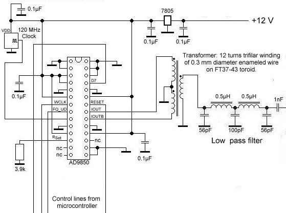
Balanced output to my experience is recommended when using Analog’s DDS chips that supply 2 output ports. Use a simple output transformer (e. g. on an Amidon FT37-43-core, trifilar wound). The transformer is followed by an amplifier. See the full scheme for this one! A low pass filter in between these two sections improves waveform and eliminates harmonics. The signal then is fed into the TX and RX mixers simultaneously. The DDS now puts out 2 Volts p-p on from 3 to 20 MHz giving a pure sine wave with flat signal levelling over the full frequency span.
Hint: If you own a spectrum analyzer you can write a simple test program to produce sine waves over the whole frequency an check the flatness of your DDS this way.
Band switching
The main thing that makes a multiband transceiver much more complex than a monobander is the neccessity to switch frequency related filters in certain parts of the circuit even if broadband designs are widely applied. There are three sections in which band switching must take place in my rig:
In the receiver section:
- At the front end.
In the transmitter section:
- At the output of the transmit mixer before first amplifier, and
- after the final stage where the low-pass filters for each band are selected.
At the low power end of the chains (front end and tx mixer) where signal levels don’t exceed 1 or 2 volts p-p several ways of switching are theoretically possible:
- Diodes as switching elements
- IC-Multiplexers
- Miniature relays
Method 1 usually involves stray capacities, so signal seperation is far from being overwhelming. Effective decoupling is a big problem with this on the other hand cheap and handy method.
Alternative 2 ensures very much a higher level of signal seperation but depends on the availability of the respective ICs needed like the 74HC4052 (a multiplexer IC) for example
Because of the fact that from a former model railraod project I still had a large bunch of 5V coil voltage OMRON relays, I decided to use these. Most relays normally tend to have good RF decoupling capabilities because capacities of the unswitched contact pairs are in the 1..2 pF region or even lower. That is absolutely OK for rf designs! Check the data sheet for exact data before buying a certain relay model.
In my transceiver the 3 relays sets for each band (receiver front end, TX mixer output and low-pass filter after final amplifier stage) are connected in series and are driven directly by 12 volts by a simple switching transistor directly controlled by a port line from the microcontroller using a small transistor driver stage (see circuit of microcontroller board). Each relay gets about 4 volts of coil voltage (then drawing about 40 mA) which is more than enough because my OMRON relays start reliable switching from a coil voltage of about 3.3 V. So the transceiver theoretically can be operated down to 10 Volts DC without any danger that the band relays might not switch correctly.
Band switch drivers
The drivers for each band that drive 3 series switched relays per band are controlled by one seperate port of the controller (Ports PE3 to PE7). PE3 is for 80 meters, PE4 for 40 and so on. BC547 transistors are enough because the 5V Omron PCB relays draw about 35 mA. Max. collector current for a BC547 is 100mA.
Measurement section for “environmental” data
A lot of values are detected with sensors in this rig. Several voltage dividers are visible on the upper left part of the scheme. They measure:
- Power supply voltage
- Temperature of the TX final stage heat sink
- RX signal level derived from the AGC
- RIT voltage
The signals are fed into the various PORTS of the ADC of the µC. Check for the software code that will be soon pageet for details.
The transmitter
I have to admit, I underestimated the diffculties that I was going to face when constructing a 3 to 30 MHz broadband QRP amplifier with a power output level of about 10 watts on all the five bands covered. I read a lot of stuff in advance, particularly the ARRL library, to get aquainted with the basics of designing linear broadband amplifiers for rf.
To make clear what I’m talking about, here’s the final and full circuit after hours and hours of testing, improving, testing, conceiving, improving…. 😉
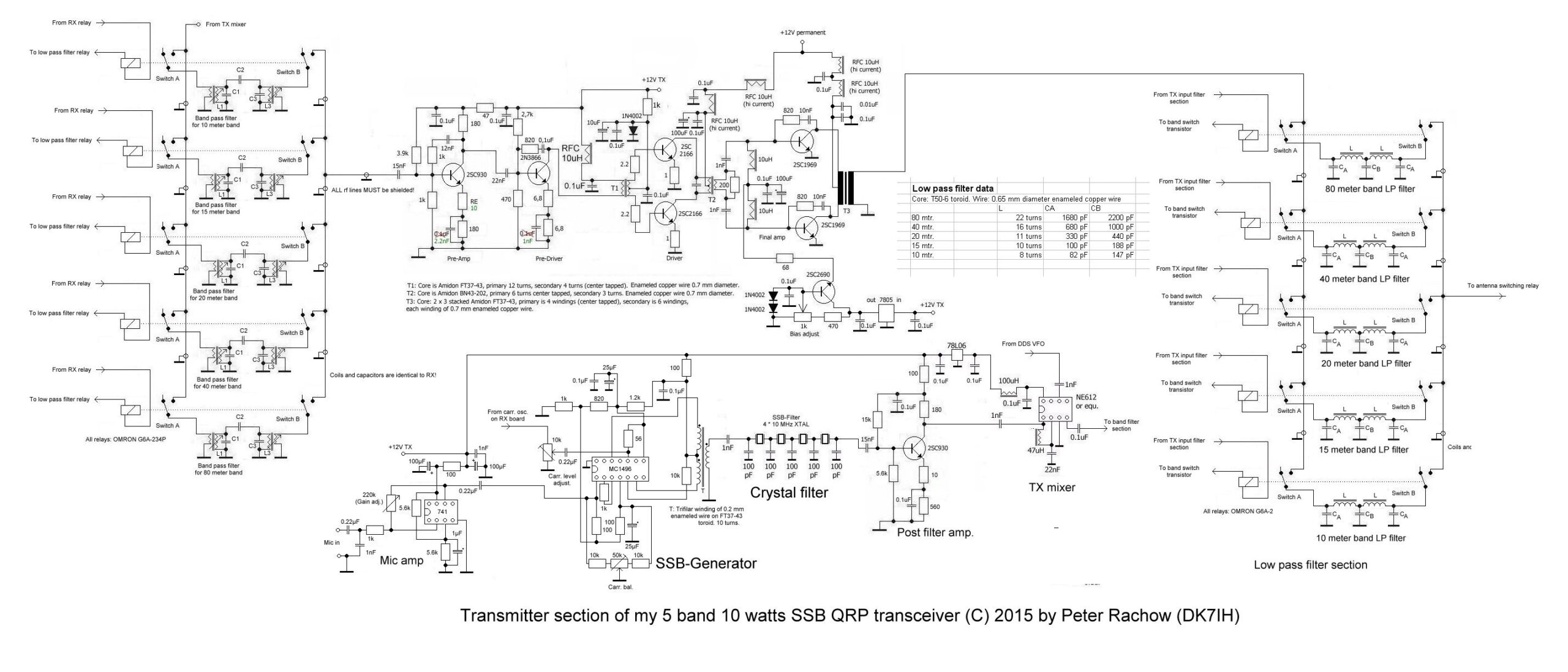
The mere power amplifier strip has, as you can see, got 4 stages:
- Preamp
- Predriver
- Driver (push-pull)
- Final amp (push-pull)
The design is capable of delivering about 20 watts of rf power but I wanted to run it within a well defined distance from its limits to ensure top signal quality. On the other hand I had kept in mind that a broadband design always offers significantly lower overall gain than a monoband amplifier. So there should always be a certain amount of gain in reserve.
You may ask why I used 2 push-pull stages. The answer is: Due to the fact that they are operated in class AB-mode I wanted to keep linearity as high as possible. Class AB amplifiers have got a relatively low standing current (bias) and therefore a higher degree of efficiency than class A. The transistor gets only a low quiescent base current, so linearity lacks compared to class A. But it does not get far as hot as his class A brother.
The solution to the bias-problem is the push-pull circuit. Each transistor of the pair now only amplifies one of the half-waves of the duty cycle. These are seperated by the input transformer and are put together again by the output transformer:
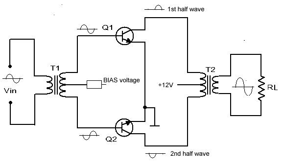
So, in contrast to a class A amp which has to be biased for amplfiying the positive half-wave AND the negative share of the waveform and thus needs a much higher bias current, the push-pull design can be operated with lower bias because it has to amplify only one part of the wave cycle which is now split by polarity into two transistors.
And, because a push-pull amp offers built-in even-harmonics suppression, the production of overtones is limited by this circuit without the need for filters.
After the amp was finisehd I did a lot of research using my old HP8558B spectrum analyzer and found that harmonic suppression is excellent as well as third order products are if you don’t use the full power capabilities of the amplifier strip.
How to make an amp broadband
The main problem with transistor amplifiers (mainly those designed for rf purposes) is the gain-vs-frequency problem. When increasing the operating frequency of such an amplifier you’re about to lose 3 dbs of gain per octave. This means, you get high amplification rates on 80 meters and a very much lower one on 10 meters. Not very nice if you want to achieve a comparable amount of gain on all the bands the transceiver is going to cover.
Next topic: I use CB transistors with a relatively high transition frequency (ft) of about 150 MHz or even higher. This means on 80 and 40 meters you can expect tremendous gain. A strong tendency towards self-oscillation and instabilties is one outcome of this situation. But on the other hand for 15 and 10 meters this high ft is a must!
So, a lot of potential problems ware waiting for the ambitious radio constructor. But, no need to get desperate: There are various cures for the various problems. To make the amp stable and clean I applied the following techniques:
- Amplifier stages are coupled by relatively low valued capacitors,
My first mistake before bypassing correctly was to try to bring monoband concepts to a broadband amplifier. Adequate emitter bypassing was one of these. First I used large capacitors in the range of 0.1µF. Much too much, as I found out later. OK, a high valued emitter bypass capacitor hands you back a lot of gain but unfortunately not equally distributed over the frequency span. It’s much better to reduce the value of the emitter bypass capacitors down to some nanofarads. You may ask: “Why is this the case?” Simple answer: The resistance of a capacitor for alternating current is given by
XC = 1/(2*Pi*f*C)
Low value capacitors thus prefer higher frequencies and attenuate the lower ones.
2. The same is true for the emitters bypasses:
The bypass capacitors lets ac flow unresitedly over the paralleled resistor.
3. In addition, negative feedback is applied to the 3 of the 4 stages to reduce gain when the operating frequency is low:
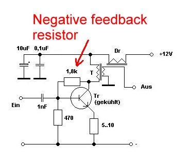
A certain amount of rf energy floats back to the base but is 180° out of phase thus compensating input energy.
4. Emitter degeneration also helps to get gain constant AND lowers distortion:

The unbypassed capacitors causes a voltage drop when emitter-collector current rises. Therefore the voltage between base and emitter lowers (base is biased to a fixed value), the gain decreases.
But, as I said before, all these measures cost a certain amount of gain. That’s why I use a 4 stage amplifier rather than a one with only three stages. The effort, by the way, paid. The waveform of the two-tone test is absolutely top on all the 5 bands. But it was a hard way to go there!
Crucial mistakes and their correction
When I tested the first version of the amplifier, I was deeply disappointed. The signals were bad, distortion was a severe problem. Also I had lots of parasetics particularly on the higher bands and self-oscillation occured as soon as I started to increase the drive coming from the tx mixer. One of the reasons for this was improper shielding of the band filter section that follows the TX mixer. I will talk about this in a later page.
By the way, don’t ask me, if the amp was “flat”. No, it wasn’t. Definetely NOT! That was the point when I began to hate this project. 😉 But then (instead of giving up) I started thinking of what I could have done wrong. Step by step I got closer to my goal…
Construction methods for the test procedures: “Plug and pray!”
To enable me to change the “critical” components like emitter bypass capacitors very fast without taking the soldering iron into my hand I use SIP socket strips:

Advantage: You can run endless tests without being endangered to seriously damage the solder pads of your Veroboard! The needed numbers of pins are cut from the strip with a coping saw or a mini cut-off wheel. Once soldered they remain in the board till the end of days. Disadvantage: If your component has thin wires, these will fall out off the socket. But for 98% of my components this works fine!
Components prone for being optimized by this method are:
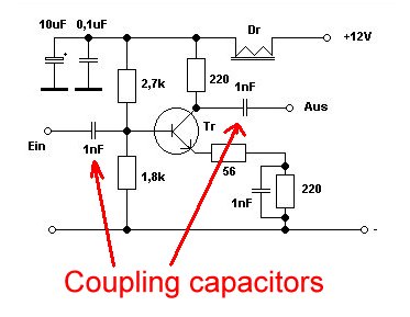
- Coupling capacitors
- Emitter bypassing capacitors
- Emitter resistors
- Negative feedback resistors and/or capacitors (whatever you have!)
Optimize your rf transformers!
RF amplifiers in high-power stages (i. e. above the Milliwatt level) usually use transformers for coupling rf energy from one stage to the next. They hereby can serve as impedance transformers, because input impedances of trasistor stages are often in the range of only some ohms whereas the output impedances of the previous stages are 4 to 10 times higher. I own a large number of my favourite Amidon toroid cores so that I can produce a variety of test transformers that can be soldered quickly to soldering nails. Again this is to avoid the repeated soldering process ruining my Veroboards:
By methods like these and 2 months of steady improvement I finally got the transmitter working the way I wanted it to have.
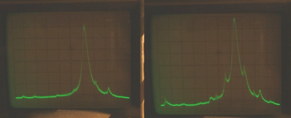
Measurement results at the completed unit:
- Output power in two-tone-test: 10 Watts at 11.9 V DC power supply
- Carrier suppression: greater than 50dB
- IMD3 products: 36dB (measured at 14,200 kHz)
Spectral analysis of output signal (f=14,200 MHz):
The receiver
Now it’s time to discuss the receiver section of my 5 band QRP SSB transceiver. The main objectives for the receiver were:
- Must be able to deal with high signal levels particularly on the 80- and 40-meter-band.
- Must be able to seperate strong out of band signals (broadcaster etc.).
- Must be able to seperate strong in band neighbourhood signals.
- Must have high dynamic range.
Here’s a brief description of the various stages of the receiver board:
- 5 relay switched 3 pole band pass filters make up the front end,
- followed by dual gate MOSFET-preamplifier and a
- diode ring mixer equipped with a diplexer,
- IF preamp with bipolar transistor,
- IF main amp with IC (good ol’ MC1350),
- product detector with 2 diodes,
- AF preamp with bipolar transistor,
- AF final with LM386.
As usual, here’s the circuit first:
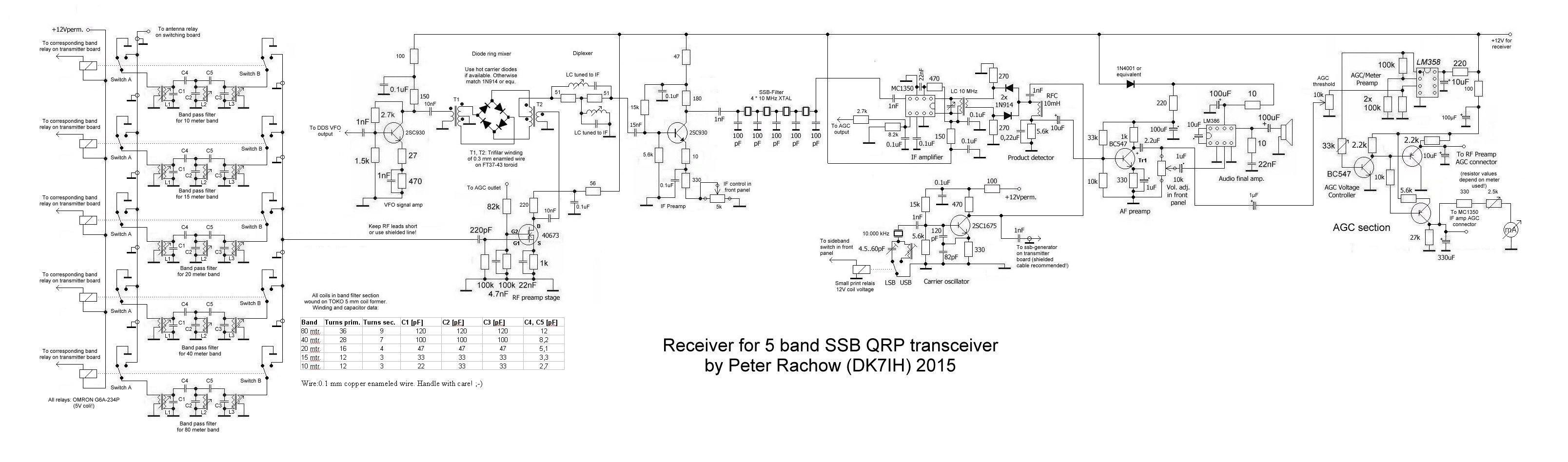
Some words concerning the various sections of the circuit:
The front end
On the left you can see 5 relay switched band pass filters. To ensure maximum out-of-band signal suppression I chose 3 pole filters. The effort is a little bit higher, I have to concede, but it’s absolutely worth. No intermodulation or other interference by strong broadcasters close to ham bands (particularly on 40 meters!) occurs.
The filter coils are wound on TOKO style coil formers of this kind. The relays are OMRON G6A-234P pcb relays. They are designed for 5 V coil voltage. Due to the fact that my rig needs 3 sections of relay switched circuitry (rx front end, band filter past the tx mixer and low pass filter past the exciter) I switched the corresponding relays for one band in series. They then are driven by 12 volts controlled by the ATMega128 driving my DDS system. The wiring of the relays is a little bit more complicated as if I had them switched in parallel but in the end this was a nice way of recycling a larger bunch of these relays that I still had on stock from a former model railroad project. 😉
Past the front end filters next stage is the well-known dual gate MOSFET rf preamp controlled by AGC.
The Mixer
The amplifier terminates broadband style (toroid transformer) putting its rf energy into a diode ring mixer which by definition is a balanced mixer circuit. The DDS VFO signal is injected on the other side of the mixer. Please note that you need a preamplfier if you run that mixer type by a DDS because the outputlevel of a DDS (if not amplified) does not suffice the 7 dbm a diode ring mixer needs for proper operation. Therefore I’ve included a small signal amp with a bipolar transistor.
To minimze spurs in your receiver it is of maximum improtance that this VFO amp works 100% linear. Keep an eye on not overdriving the amplifier! Any signal level beyond linear operation condition produces spurious emmissions. If available check the output with a spectrum analyzer! Reduce input voltage by inserting a voltage divider made of resistors (not capacitors!) if input level is too high!
A diode ring mixer also needs to be accurately terminated to 50 Ohms for optimized performance. Thus I’ve added a diplexer after the mixer which ensures an adequate termination of the mixer on the IF frequency.
IF and AF stages
Next steps are an IF preamplifier (which is connected to a manual gain control potentiometer sited in the front panel), a ladder filter with about 2.4 kHz width and the IF main amp equipped with MC1350 by Motorola. The IF amplifier IC is connected to the AGC strip at the end of the receiver section.
The succeeding diode based product detector is fed by the amplified IF and by the carrier oscillator which is also sited on the receiver circuit board.
An audio preamp and the LM 386 as the power amp do the final job of amplifiing of the audio signal together to loudspeaker level.
The audio-derived AGC circuit is the same like in my hand-held transceiver. Two dc outputs are available. One delivers increasing voltage when signal strength is rising, the other decreases voltage under the same condition. The first one is about to control the MC1350, the later one is for the dual gate MOSFET that can be found in the receiver’s front end.
Here, for the final, is an overview of the receiver board in my 5 band QRP SSB transceiver. Thanks for reading!
First QSOs went very fine on 20 meters where my antenna is tuned to. Let’s see what the rig will show the next weeks, I’ll keep you informed. Please watch later pages on this blog that will show adaptions and modifications of this rig. 😉
73 de Peter (DK7IH) and thanks for reading!
On the transmitter schematic you left out the value of the capacitor across the primary of T2.
Oh, yes you’re right. In the meanwhile I’ve removed that C again because signal quality improved. I blew one of the original Motorola 1969ers due to overheatuing (a VERY long test run and insufficient cooling were the reason) and installed 2 replacement 1969ers made by ELEFLOW. These delivere more power and a cleaner signal so that C was made redundant.
73 de Peter
I was thinking of duplicating that power chain using Motorola MRF475 output transistors and MRF476 as drivers, as I have these in the junk box. Your circuit looks similar to the Motorola AN779 ap note.
Yes, seems to be so. 😉 But the approach is a general one. And AN779 follows this. I used push-pull-driver and push-pull final stage to achieve optimized linearity in the class AB stages of the transmitter. This is only given to the maximum extent if you use a push-pull design. Therefore my circuit might resemble AN779 application note. 😉
A QRP SSB multiband transceiver for 5 bands The coil using on receiver side
LC tune to IF. What coil is that
The coil is 20 tuns prim. and 5 turns secondary on a small TOKO coil former. Parallel capcitor is 56 pF for 10MHz IF.
vy 73 de Peter
By the way,
before Band Pass Filter, i have been constrained to placed a LNA circuit (bfr91a) because without lna the receiver was so weak. But when i put a lna circuit, the receiver become an excellent one.
May be i couldn’t find your dual gate fet. Instead of yours i used BF961 so may be this fet is not sufficient one.
I used AD9850 DDS. Pretty good result one. 73
Which is the cost of this transceiver 80-10 mt? And why you haven’t introduced the 160 mt?
Hi,
total costs are all in all 200 to 250€, depending on what you already have in your scrap box. 😉 And I didn’t integrate 160 because I don’t have a suitable antenna for this band.
73 de Peter
Are you available to build a qrp transceiver for me which covers 40 meters?
80-75-40-20-17-15-12-10-6-4-2-70cm?
Hi there,
sorry to say so, but my activities are strictly non-commercial since my occupation takes 100% of my working time. Amateur radio is just a hobby besieds my professional activities.
73 de Peter
I made 5 band project. it works perfectly, but with a difference, after front end 3 adjustible coil filter, i had to placed a LNA (low noice amplifier) has one transistor. Because dual gate fet was not sufficent. Now it is okay.
I want to send you a youtube video of my “prototype” receiver: Thank you share this project.
https://youtu.be/riEo4jzHUW4
Yes Peter, ofcourse i will try to put it into a cabinet, but it is more hard to put it into a cabinet than to make an elecronic circuit. TX Exciter also is okay. That is; LM741+ MC1496+NE602 content SSB circuit is working well, second portion is filter and Power Amplifier is also working well, but PA is not your circuit.
Happy new year & Marry Christmas 73
Another video:
https://youtu.be/gSkgL8nQTx0
You can share your project Atmega program. “Give me FIVE!” – A QRP SSB multiband transceiver for 5 bands with 10 Watts output power. I started to work with your arms to make your device work. 73’s
TA2ITA
ad9850 dds vfo Atmega 128 programs.thank you very much.
Hi! The code for AD9850 was just for test purposes. I soon rebuilt the DDS with an AD9951. I will mail that to you. 73 de Peter
Edit: I could not get the e-mail address out of your post, so I created a new post to this blog. Enjoy! 73 de Peter
can you send me 5 ssb mutiband qrp hex code? TA3USC 73.
No problem, but you must send me your E-Mail address first to peter.rachow@web.de
73 de Peter
Peter,
I drowed a pcb by using dip components for 5 band rig. it was working well, but signal gain was very weak. to strenght it, I applied a LNA between filter and fet. Yesterday, i discovered that, the DDS aplifier transistor design does not amplifiy the signal of VFO. Resultant signal strenght is the same inlet signal. But transistor is not faulty. I tryed to cancel emitor resistors, and connect emitor directly to GRAUND. Ohh my god… the signal amplified 10 times, according to my oscilloscop. And receiving signal increased too much. now no need LNA.
I mean, the DDS amlifier section should be wrong designed? Thank you.
Hello Dündar,
thanks for your reply. I don’t think the design is wrong because I have used it frequently for other transceivers and it can be found in a similar way on all kinds of rf amplifiers.
The only thing with my circuit is, that the emitter resistor with 560 ohms is a little high (usually people use 100 to 200 ohms). But this was because the amplfiier in my circuit put out too much voltage so that it overdrove the rx mixer leading to low IMD3 performance.
What type of transistor are you using?
vy 73 de Peter
Peter,
I drowed a pcb by using dip components for 5 band rig. it was working well, but signal gain was very weak. to strenght it, I applied a LNA between filter and fet. Yesterday, i discovered that, the DDS aplifier transistor design does not amplifiy the signal of VFO. Resultant signal strenght is the same inlet signal. But transistor is not faulty. I tryed to cancel emitor resistors, and connect emitor directly to GRAUND. Ohh my god… the signal amplified 10 times, according to my oscilloscop. And receiving signal increased too much. now no need LNA.
I mean, the DDS amlifier section should be wrong designed? Thank you.
Peter, thank you for fast reply. I used 2n2222 , bu you offer 2sc930. May be if find this transistor i replace it instead of 2222.
Also transmitter section, 741-mc1496-NE602 tripple section, i can say “exciter” is so sensible & produce a very very perfect SSB signal. In my oscilloscop, the ssb signal, mc1496 signal suppression & modulation is perfect. Again thank you for this exciting project.
Hello Dündar Yasa,
the 2N2222 is OK for this purpose. Then the only thing that I can imagine is that there might be a defective component in the emitter line or a faulty soldering. The amplifier works well within half a dozen of my constructions.
What you can do: Bridge the 10 Ohm resistor and change the 560 to 100 Ohm. Then gain must be in the range of 10 to 12 dB if the circuit is OK. Maybe you can check that an give me a reply.
vy 73 de Peter (DK7IH)
Peter, my amplify transistorfor of VFO frequency is 2n2222.
But I’ll try to find your 2sc930 transistor, otherwise, try to decrease the values of emitor resistors, instead of connect directly to the ground. It is not through to connect directly emiter to the ground I guess.
By the way, can should be the Chinese resistor’s value different than write-on it? so, the giant value blokage the transistor?
It was good to conversation with you Peter. I’ll try & write you the result from this page. 73 from TA3IHD
Hello Dündar, Yasa, maybe you can check the resistor with an ohmmeter. I found that metal film resistors are hard to read concerning the color code on them. Carbon resistors are much easier to recognize. vy 73 de Peter
BTW: Don’t search for the 2SC930, it is just hard to find. 2N2222 is very much OK! 73 de Peter
Hello Peter, I just realised a DDS AD9951 with a PIC18F controller code in PICBASIC. It’s working but level is not that high… -9dBm from 1.8 to 30MHz. So I’m really interested to make a small QRP amplifier. As I don’t want more than 30 to 33dBm, and as i have 2 2SC2166 in stock, I wonder how to make your amplifier without the last amplifier stage (2x2SC1969). I would like to understand how to know the Z out of the 2x2SC2166… And how to match to 50Ohms broadband at this point (output). This will be a fabulous lesson of HF techniques for me. Can you help/explain ? Best regards and 73’s F1SLU Hervé
Hello Hervé, thanks for your entry. Here are some thoughts on the topic you mentioned:
You require an output level of about 30 to 33dBm. With 50Ohms antenna impedance, that means your transmitter must have 1 to 2 watts output. I think a push-pull final with 2 2SC2166 is ab little bit “overkill”. I would recommend a single ended amplifier instead.
Output Z calculation can be done by calculation or on an experimental basis.
First you can use the following formula:
Z = VDD²/2*Pout.
This will give you an approximate value in a given range of uncertainty for output impedance. The problem is that you must take into account the windings of your output transformer and the respective ratio of primary vs. secondary windings if there are any.
Another method uses a more experimental approach: You connect the input of the transmitter to a signal generator (or the DDS in your case). The TX output will be terminated with a non-inductive resistor. This resistor is changed during the experiment in steps. I usually start with 20 Ohms and then increase the value of R to let’s say 70 ohms in steps of 5 to 7 Ohms depending on the resistors available.
For each resistor I measure the output voltage (rms) with a VTVM and rf probe attached. Afterwards I calculate the output power (P = Vout²/R). When entering this set of values (R -> Pout) to a spreadsheet (or a paper if you prefer the classical method 😉 ) you will get a function with a peak. That is max. output power. Due to the fact that you will get max. PWR when input and output impedance match you can see the output impedance of the transmitter.
This can be done theoretically with any transformer. All you have to know is the winding ratio. The impdedance transformation then is squared. A 1:2 winding ratio will result in a 1:4 impedance ratio.
vy 73 de Peter (DK7IH)
Thank you for reply, Peter. I remember now the formula: Z = VDD²/2*Pout . OK, so if the output power of a 2SC2166 is about 3Watts then Z = 24 Ohms. If I understand, I need a transformer 1:2 to match 50R in a single 2SC2166 amplifier. Is it correct ? Unfortunately I talk about 1-2 watts but this is not a good choice if I want to drive another amplifier (5W input) So… a pair of 2SC2166 will be the good choice. Question: For this new (same as your schematic) stage and if now Z output = 12R, I need 1:4 transformer in place for T2 (connected like T3). Do you have any link to help me to make this kind of transformer (covering 160 to 10m) ? May be, could you explain the way you make your T1 transformer ? Thank you very much. Hervé
Hello Hervé, for T1 I would start with a 12:6 ratio and also would build a 12:8 transformer and then check out which one performs better. This is because the calculation only is approximate. For T2 (1:4) I’d use 2 turns primary (center tapped) and 4 turns secondary. As a test I’d also build a transformer with 5 turns sec.
I found out that it is a good idea to have a larger numbers of toroids on stock so that you can build alternative transformers and then check out which one is best.
And, sorry to say, I don’t have a web resource on transformers because I did all the experiments on my own getting started with values from existing transceivers.
vy 73 de Peter (DK7IH)
Nice I am waiting for the pcbthank you.
Please send E-mail to dk7ih@yahoo.com and I will send the HEX-File! 73 de Peter
Peter i had to written before about dds amplifier for rx.
The transistor was not amplify enough & was ground emiter so then amplify the signal.
But in that case, transistor heates much.
When i increased value of emiter capacitor from 1n to 10n the result was perfect.
It amplifys the signal from 2v to 5v on oscilloscop.
I obtain on tx perfect ssb signal on ne602. But my power transistors was all fake. So didn’t amplify that weak ssb signal.
Now wait the genius trsnsistors to make pa.
Dündar YASA
TA3IHD
Peter,
In tx section, after ne602 ic, there is a group of two coil filter.
Between two adjustible coil, there are transition capacitor “C2”. For 20 & 40m band, what is the values of these capacitors?
Thank you from TA3IHD 73.
Hi, for 20m use 4.7 pF, for 40m 6.8 pF. Or one standard value up or down. Vy 73 de Peter
Thank you Peter.
TA3IHD 73
You are always welcome! 🙂
😊😊
hi ,
Since I do not have access to the main components, such as FT 37-43 to make the diode mixer transformers that you used in your circuit, I used the core of energy-saving lamps whose inductance is greater than a FT 37-43 core. Does it have a great effect on circuit performance? Can I use this core? The value obtained for 9 turns of the wire 0.3 mm is about 150 microns, how much inductance of the coil can be tolerated for different frequencies
Thank you for your guidance.
Hi Fariborz,
with 150uH on your specific core you are very close in the region an FT37-43 will be. As I have just measured with a test core, 10 windings on this FT-37-43 core result in L=120uH. Without exactly knowing the specs of your core, I would just say: “Give it a try!” 🙂
vy 73 de Peter (DK7IH)
Bonsoir peter;
Je suis attentivement depuis longtemps votre site hamradio et je vous remercie pour toutes vos publications.
J’ai regardé la page de vos kits et sur le schéma du SSB modulator MC1496N(2022), je pense que la sortie de la résistance de 820 ohms n’est pas câblée correctement. Je l’ai déconnecté au niveau du noeud de la capa de 10µf et raccordé sur la ligne verticale 2X100, 1k et 0,1µf.
Est-ce que je me trompe ?
Merci encore pour vos montages qui nous permettent à nôtre RC F5KEI de longues discutions et de bonnes réalisations
Bonjour, Jean-Pierre, merci beaucoup, tu es absolument correct et j’ai me trompé. J’ai corrigée le plan sur mon website. 73 de Peter (DK7IH)
Bonjour Peter, merci pour la réponse, je parlais du schéma sur la page : “kit SSB modulator.
Autre question Quartz 9 Mhz ou se fournir ? en fonction des caractéristiques du quartz
73 f5etm
Bonsoir Jean-Pierre, j’ai t’écrit une e-mail….
73 de Peter