This is a software project for building a VFO with the 75MHz clocked AD9834 synthesizer chip by Analog Devices. Due to the Nyquyst theoreme with a maximum clock rate of 75 MHz a frequency of 37.5 MHz can be achieved. When overclocking the chip to 100 MHz (which has been succesfully tested in many cases) the maximum output frequency theoretically rises up to 50 MHz. But when coming close to these boundaries signal quality deteriorates severely. So it is recommended not to produce higher output frequencies than 25 MHz (75 MHz clock) or respectively 33 MHz (100MHz clock).
Theoretical outline
The AD9834 is a low power (20mW power consumption when VDD=3.3V) DDS module. It can handle up to 5.5 V as VDD (2.3V min.), so 5V single supply use makes circuitry simple. It comes in a 20 lead TSSOP case, breakout boards are available.
SPI signal structure
Programming a desired frequency into the DDS chip is performed by a 3 line communication, a serial peripheral interface (SPI). These three lines are called
- SCLK (the clock signal)
- FSYNC (the signal that determines the end of the transfer of a single word (16 bits)
- SDATA (the frequency or control information packed in 16 bit word)
The timing diagram found in AD’s datasheet gives the precise structure of the signal communication:
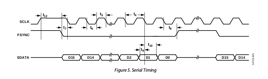
FSYNC is high when the first word (16 bits) is going to be transferred. SCLK is also high in this moment. Then FSYNC is set low, 16 bits subsequently are transmitted via the SDATA line. After one bit has been transmitted, SCLK is set low for 10 ns minimum and then goes high again for the next bit. Transfer starts with MSB (D15).
After 16 bits have been transmitted, FSYNC is set high again, showing the DDS chip that the word has been completely transferred. As soon a FSYNC is low again the DDS is ready for the transmission of the next 16 bits.
The DDS chip “language”
Frequency set
The chip has two frequency registers (FREQ0 and FREQ1). These registers contain 28 bits of frequency information. They can be addressed individually and are divided into two 14-bit sections each (MSB and LSB). In addition it is possible to load the LSB independently from the MSB if only a minor frequency change is required.
Frequency registers are selected by the first two MS-bits (DB15 and DB14) of a 16 bit structure sent to the DDS. “01” determines a frequency load for FREQ0, “10” loads the FREQ1 register.
Control transmission
Besides the frequency information some controls must be sent to the DDS chip. A control is also 16 bits wide. A control is initiated by a “00” starting sequence for DB15 and DB14.
Summary
So we can distinguish the purpose of a word by its first two bits:
- “01” + 14 following bits loads the FREQ0 register,
- “10” + 14 following bits loads the FREQ1 register,
- “00” + 14 following bits transfers a control word.
One important control bit under the looking glass
There are many features to control the AD9834 chip. We want to limit this to the absolute basics. The most important bit is DB13. If you set this to “1” the chip is informed that the frequency information for the register to be loaded next will come in two consecutive 16 bit words addressing the respective frequency register with the 14 + 14 bits of frequency information.
So the first step is to transfer the “00” signaling a control code and next the “1” signaling that the user wants to write two 16 bit words for changing the frequency. The rest of the 16 bits of this control can be left “0”. This results in
“0010000000000000” (0x2000)
is the first word to be transmitted.
Frequency calculation and transfer
The frequency data of the waveform the user wants the chip to put out is determined by 28 bits, a so called “frequency word”. The formula is
frequency word = 2^28 / fclk * f
- frequency word: a floating point number that will later be converted into a long integer containing the frequency information for the chip,
- fclk: The master clock rate of the clock oscillator connected to the DDS [Hz],
- f: The frequency the user wants to be generated [Hz].
Example
With a clock rate of 75 MHz a user frequency of 1 MHz would be calculated as a frequency word of
268435456 / 75000000 * 1000000 = 3579139,413333333
By leaving only the integer part of the number we get 3579139 which now is the frequency word that must be transferred to the chip.
Converted to binary this number figures out as
00001101101001110100000011
This is now split into two parts, 14 bits each:
0000110110100 1110100000011
Now we must tell the DDS in which of the two frequency registers we want to store this. Therefore we add the 2-digit-code for the desired frequency register in front of the respective number. In this example the destination is FREQ0, so we add “01”. The result are two words of 16 bits each:
010000110110100 011110100000011
Together with the control that allows us to write the 2 words consecutive into the chip we get a complete sequence of
0010000000000000 011110100000011 010000110110100
because the correct order is CONTROL first, then LSB, and MSB last. In HEX this is 0x2000, 0x3D03, 0x21B4.
Coding
Code examples in C for the AVR family follow. First the declarations, then some defines in advance so that you can adapt the code easily to your layout:
//Declarations SPI for DDS
void spi_start(void);
void spi_send_bit(int);
void spi_stop(void);
void set_frequency2(unsigned long);
// Defines SPI DDS (AD9834)
#define DDS_PORT PORTC
#define DDS_FSYNC 1   //PC0
#define DDS_SDATA 2   //PC1
#define DDS_SCLK 4    //PC2
#define DDS2_RESETPIN 3  //PC3
Before a transfer starts we need to send a “start” command to the SPI to set SCLK and FSYNC adequately. This is coded as:
void spi_start(void)
{
    DDS_PORT |= DDS_SCLK;     //SCLK hi
    DDS_PORT &= ~(DDS_FSYNC); //FSYNC lo
}
After a word has been transmitted this mus be shown with the “stop” command to inform the chip that 16 bits have been sent. So we set FSYNC to high:
void spi_stop(void)
{
    DDS_PORT |= DDS_FSYNC; //FSYNC hi
}
With these two functions we can initiate and terminate the transfer of 16 bits of data to the chip.
Next we must learn how to transfer data. This will be done by sending just one bit to the DDS and afterwards switching the clock accurately:
void spi_send_bit(int sbit)
{
    if(sbit)
    {
        DDS_PORT |= DDS_SDATA; //SDATA hi
    }
    else
    {
        DDS_PORT &= ~(DDS_SDATA); //SDATA lo
    }
    DDS_PORT |= DDS_SCLK; //SCLK hi
    DDS_PORT &= ~(DDS_SCLK); //SCLK lo
}
And now for computing and sending the frequency word:
void set_frequency2(unsigned long f)
{
    double fword0;
    long fword1, x;
    int l[] = {0, 1, 0, 0, 0, 0, 0, 0, 0, 0, 0, 0, 0, 0, 0, 0};
    int m[] = {0, 1, 0, 0, 0, 0, 0, 0, 0, 0, 0, 0, 0, 0, 0, 0}, t1;

    fword0 = (double) 3.579139413 * f; // 3.579139413 = 268435456 / 75000000
    fword1 = (long) fword0;

    //Transfer frequency word to byte array
    x = (1 << 13); //2^13
    for(t1 = 2; t1 < 16; t1++)
    {
        if(fword1 & x)
        {
            l[t1] = 1;
        }
        x >>= 1;
    }

    x = (1L << 27); //2^27
    for(t1 = 2; t1 < 16; t1++)
    {
        if(fword1 & x)
        {
            m[t1] = 1;
        }
        x >>= 1;
    }

    //Transfer to DDS
    //Send start command
    spi_start();
    for(t1 = 15; t1 >= 0; t1--)
    {
        spi_send_bit(0x2000 & (1 << t1));
    }
    spi_stop();

    //Transfer frequency word
    //L-WORD
    spi_start();
    for(t1 = 0; t1 < 16; t1++)
    {
        spi_send_bit(l[t1]);
    }
    spi_stop();

    //M-WORD
    spi_start();
    for(t1 = 0; t1 < 16; t1++)
    {
        spi_send_bit(m[t1]);
    }
    spi_stop();
}
I use a set of 2 arrays as predefined words including the start sequence for FREQ0 and then writing each single bit into the respective array.
To start the DDS correctly a short reset sequence should be placed in your main()-function:
//Reset DDS (AD9834)
_delay_ms(10);
DDS_PORT |= (1 << DDS_RESETPIN); //Bit hi
_delay_ms(10);
DDS_PORT &= ~(1 << DDS_RESETPIN); //Bit lo
_delay_ms(10);
Alternative: Tie the RESET-Pin of the AD9834 permanently to GND. Notable that also a software rest is possible, but I prefer the hardware method.
By set_frequency(Value) you can start using this DDS.
73 de Peter (DK7IH)