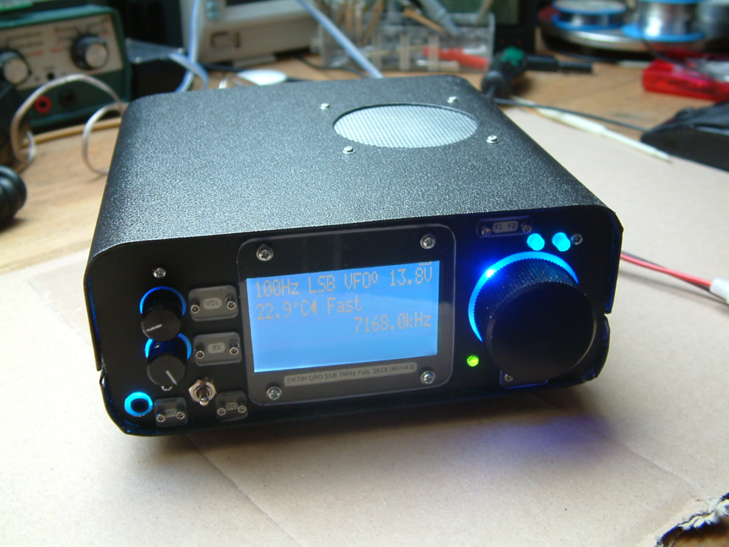
After having done lots of QSOs with the 7MHZ QRO transceiver I found that the receiver still had to be improved. The sensitivity was great, the sound also was but there were some difficulties when operating the radio during evening and night times because some (minor) interference was audible. This symptom had been caused, as usual, by strong broadcast stations transmitting from 7200+ kHz 41m-band. Occasionally “Radio China International” and “Radio Romania International” were discernable. But cure was on the way: The transceiver has a modular concept. Based on this I decided to do a full reconstruction of the receiver module.
The mixer, which is the most crucial part in a 7MHz receiver was changed to an IC mixer using an SL6440 double balanced mixer (formerly produced by Plessey).
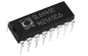
The mixer IC offers a very good IMD3 performance (30dBm maximum according to datasheet) plus some decibels (1 to say exactly!) of gain and thus is a good alternative to the dual-gate MOSFET I had used before.
As a special feature there is an input (pin 11) where a current can be applied that determines the overall mixer current. The higher this value is set, the better the IMD3 performance will be. Max. power dissipation for the IC is 1.2 watts but that will require a heatsink. I found that a resistor of 820Ω will lead to a current of 4mA (13V VDD) on pin 11 line and produces good performance without thermally stressing the IC. For optimized IMD3 performance the SL6440 ic should be run in balanced mode.
The receiver schematic in full:

Circuit explanation
Input BPF
From the left we start with a two pole band filter for 7 MHz. LC coupling again is very loose what reduces the receiver’s tendency to overload.
Receive mixer
Next is the SL6440 mixer ic. Input and output are equipped with broadband transformers (data see schematic, please!). The purpose is to convert an unbalanced signal to a balanced one and vice versa. According to the respective entry in data sheet running the mixer in balanced mode enhances performance. Pin11 is used to control the DC operating conditions of the mixer, a resistor (820Ω) sets appropriate bias for mixer stage. The 3 diodes (1N4148) supply correct voltage to a pin that is called “VCC2” which should be slightly lower than VCC supplied to the output stage. 3 diodes in series produce the required voltage drop.
In experiments it has turned out the even when gain of the mixer ic is only about 1 dB the resulting output of the whole receiver is higher than that of its predecessor and taking into account that receiver generated noise is not a problem on the lower short wave bands, there is no rf preamplifier.
If you encounter birdies maybe the signal level of the VFO is too high. Then switching a smaller capacitor into the VFO signal feedline is the best idea.
Next stage is the filter switch that has been copied from the previous schematic.
Interfrequency amplifier
This stage contains the well-known MC1350 by Motorola. To simplify this section a minimum design has been chosen, Output is unbalanced and broadband. Input also. The only filtering in the whole interfrequency section is done by the SSB filter prior to the interfrequency amplifier. A 100uF capacitor in VDD line helps to suppress audio frequency feedback and self-oscillation in the receiver strip.
Product detector
As you might have realized the transceiver not longer is a “NE602 free zone”, because this mixer now serves as a product detector. A type of usage where the low IMD3 performance does not matter. The low pass filter by the end of the mixer must be chosen according to the user’s preferences concerning pitch and tone.
Audio amp section
Audio preamp is again an ic, the “antique” LM741. Negative feedback has been set to an amount that there is significant gain in this stage (R=330kΩ).
The audio final amp here has been equipped with the TBA820M integrated circuit, the smaller version of the 16 pin TBA820 integrated audio amplifier. The advantage of this ic compared to LM386 is lower distortion and the fact that this ic is not so prone to self-oscillate.
AGC
Automatic gain control nearly is the same like in the former version. The main difference is that MC1350 needs positive voltage to reduce amplifier gain. Thus the output has been punt into the emitter line. The problem when using an NPN transistor in such a circuit is that maximum voltage is limited to Vmax = VDD – VBE. As a consequence you can not get full 12V out when you supply 12V between C and E. Here this does not matter because AGC significantly reduces gain already when reaching 6 volts (Source: Datasheet):
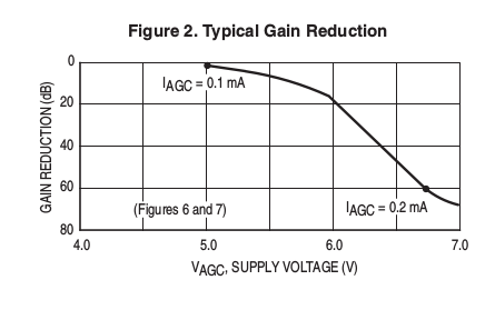
Maximum gain reduction (>60dB) occurs between 6.7 and 7 volts.
Also a manual method to reduce gain has been applied. This is by chosing a voltage between 0 and 12V using a potentiometer. To prevent current flowing from the center of the potentiometer into the ADC input detecting the AGC voltage a silicon diode has been installed. To prevent a short circuit of the AGC voltage against GND when the potentiometer is at 0 position (delivering full gain in the MC1350 amp ic) the 5.6k resistor is used.
Changing time constant can be achieved by a second capacitor set in parallel (either by a switch or by microcontroller).
To protect the analog-digital-converter (ADC) in the microcontroller from excessive input voltage, this is limited to 5.1V by a zener diode.
Performance
The receiver is very sensitive. Reception is possible with the famous “wet finger” ;-). With a large antenna (full sized delta loop) no overload is detectable even during evening and night times. Noise is slightly higher compared to that with the MOSFET equipped receiver but very much acceptable for a 7MHz receiver.
73 and thanks again for watching!
Peter (DK7IH)
The SL6440 seems to be somewhat hard to source, I found one supplier in the UK that had them on ebay, along with numerous sellers from Honk Kong or China. I try to avoid buying IC’s from China because of the risk of getting counterfeits (though PayPal will usually go to bat for you, but you have to figure out the problem quickly).
Have you tried using an H-mode mixer with FSA3157’s? You don’t really need to use the expensive MiniCircuits transformers, you can wind your own on FT-37-43 cores (a-la PA3AKE). Just try to make all three transformers identical by winding from the same prepared length of twisted wire pair. A simple 74HC04 squarer will do driven from a DDS, and the square wave output of an Si5351A may be clean enough on its own. These mixers have very good IP3! A diplexor on the output may be necessary, but a simple one with 5R1 resistors two toroids (T-25-2’s) and two 1-5% capacitors is good enough.
I wonder why you’ve abandoned using the si5351A. It seems to have fewer spurs than most DDS chips, and acceptable phase noise (maybe not as good as the AD995x series). It can also provide both the VFO and the BFO/carrier oscillator outputs. (using all three outputs can result in more spurs and jitter as two of them share a PLL, and you have to make use of fractional dividers).
Hi there!
You are right concerning the availability of the SL6440. I found one vendor in Germany who sells them for reasonable prices (5€ each) and does not deliver fakes. So I gave it a try because the IC’s wiring is simple. I have not tried the other mixer concepts yet but have made good experience with homemade diode ring mixers. That would have been the second opportunity if I had not come across the SL6440.
About the Si5351: Yes, I’m a little bit away of it. ;-)) I bought some 400MHz oscillators from Mouser and currently am exploring the capabilities of the AD9951 clocked to full extent. With the Si5351 on the contrary I found more spurs than probably you, thus I’m a little bit disappointed. With the 7MHz QRO TRX I had an Si5351 test oscillator (thanks to the modular design!) and found many more spurs than with the AD9834 oscillator I’m currently using.
One crucial thing, by the way, is the post-DDS amplifier. Many spurs are not generated by the DDS itself but by intermodulation process in the post DDS amplifier. Here careful desigg is mandatory and will get you rid of the most “birdies”.
vy 73 de Peter