Abstract
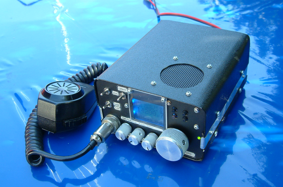
A general and good practice in engineering is a steady process of improvement. This article describes the construction of a high performance transmitter/receiver for SSB (voice) communication covering the 14MHz (20 meters) high frequency amateur radio band.
Various modules that have proven high performance, liability and ruggedness in recent constructions will be combined to form a radio with outstanding receiver performance, an ultra linear transmitter with output range 15 to 20 watts and a top audio sound quality both on transmit and receive.
Key features are:
- Dual DDS frequency generation with AD9834 (Local oscillator) and AD9951 (VFO),
- Microcontroller (MCU): ATMega644P by ATMEL,
- Single conversion superhet receiver with 9MHz interfrequency (IF) and preamplifier, mixer and IF amplifier equipped with Dual-Gate-MOSFETs,
- Audio-derived automatic gain control (AGC),
- Transmitter with MC1496 as double sideband (DSB) modulator and NE602 as transmit mixer,
- power transimitter with 4 stages, final stage in push-pull mode.
Another version of this radio has been built before. But this one was equipped with a variable frequency oscillator (VFO) because of nostalgia reasons. Unfortunately a VFO lacks certain features (frequency stability above all) which can be overcome by using digital frequency synthesis without losing performance. Usage of a high performance DDS systems is a prerequisite to achievement and a possible solution.
Most building blocks of that respective radio have been redesigned except the VFO section that turned out as not being able to deliver the projected frequency stability to a 100% degree. Frequency instability occurred because of the flatness of the former cabinet that brought the aluminum case too close to the VFO tuned LC circuit. Aluminum has a huge tendency to expand under the influence of heat so the rig was very temperature sensitive. That undeniable fault lead to a complete reconstruction using the old RX and TX modules and building a new set of frequency generators.
Parts of the old cabinet were reused but because of the fact that the whole rig got increased vertical expansion, the cabinet was “stretched” with two lateral strips of Aluminum.
Also a full electronic transmit/receive switch with p-channel power MOSFETs has been designed to avoid usage of a DC switch relay and get a “smooth” switching.
Another objective of this radio was to get out the absolute best performing circuits of the recent projects and to build a real high-performance radio. Hence this transceiver is also some sort of an improvement of the “Old school SSB TRX” as well. The circuit empirically turned out to be very good for communication in the 14MHz band. Because of this frequent readers of this website might detect certain similarities. 😉
The Receiver section
The design objectives were:
- Low noise (achieved by using Dual-Gate-MOSFETs with the receiver to a large extent)
- High dynamic range (achieved by using a Dual-Gate-MOSFET as receive mixer)
- High AGC range (achieved by taking RF preamp and IF amp into the AGC chain)
- Good audio quality (achieved by using a TBA820M as integrated AF amplifier circuit and a 5 cm loudspeaker)
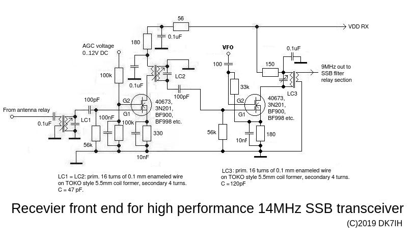
RF preamplifier and receive mixer
The radio frequency preamplifier has been designed primarily to improve the receiver’s noise figure. Delivering additional gain only is relevant in second order.
Preselection is performed with only one tuned circuit int G1 line. The center frequency of this circuit is 14.180MHz. In the output section of the stage an another identical LC circuit has been installed. This turned out to be sufficient because there is no immediate need of higher preselection. The subsequently placed mixer, that is also equipped with a Dual-Gate-MOSFET has very good high level processing qualities. No interfrequency feedthrough could be observed with various antennas. No IMD occured even when signals were very strong. Testing out in the field with partable antenna very far from man-made noise sources the receiver was very quiet and even very weak stations could be received and read with Q5.
To get most of gain swing from AGC the preamplifier is controlled by a DC voltage between 0 and 12V supplied by the AGC control stage to be described later. This voltage is halved by a 1:1 resistor voltage divider because maximum gain of the Dual-Gate-MOSFET occurs with about 6V DC applied to G2.
Clipping diodes that are sometimes used to prevent high voltage entering the 1st stage have not been installed because they are prone to produce unwanted IMD products if signal levels from the antenna are too high and undesired mixing takes place there.
To prevent self-oscillation in the preamplifier, the tuned circuit LC1 and LC2 are connected together in a special way. G1 is connected to the tuned section of LC1. This section has high impedance, thus it should be connected to a load which also has high impedance. The coupling section of the coil with low impedance is connected to the 50Ω antenna. There are not two tuned parts of the LC circuits together in one stage.
The output of the Dual-Gate-MOSFET (low impedance) is connected to the coupling winding, the high impedance tuned part is going the high impedance of G1 of the mixer. The impedance ratio between the two coils is 16:4 due to the winding ratio of 4:1 of the coil set.
The sensitivity and noise figure of the whole receiver is determined by these two stages. Measurements showed that the minimum discernable signal is about 0.1µV which is very good for a short wave receiver.
SSB-Filter, IF amplifier, Demodulator, AF amp and AGC
The following stages are some sort of best practice combination of circuits that have proven to perform very well in the recent projects.
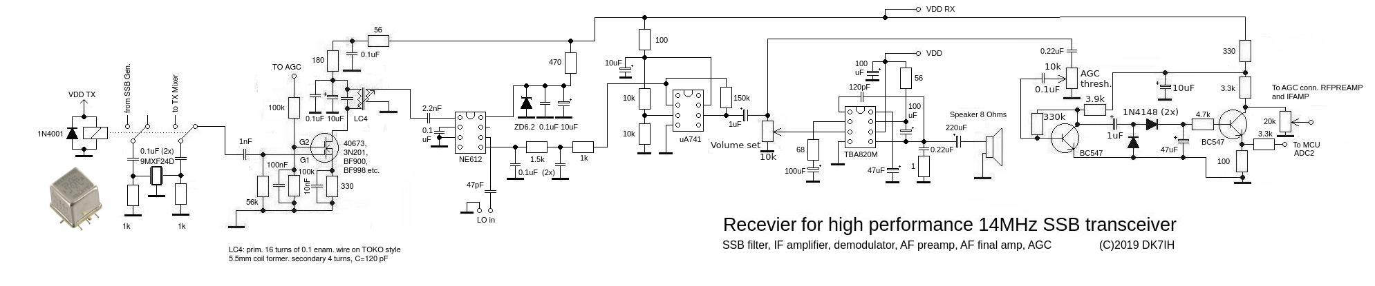
SSB-Filter and relay
The SSB filter is switched with a special rf relay by Teledyne® ensuring excellent isolation of relay ports with very low capacities in the unswitched signal path. Here the usage of shielded cable is mandatory for connecting the relay/filter section to the transmitter (see later text!). A clamp diode has been installed to eliminate high voltage peaks due to self-induction when the relay is switched. This will prevent the MOSFETs in the switching unit from excessive voltage and possible destruction.
IF amp
A proven and reliable circuit can be found here as well. One stage delivers IF gain of about 12dB which is sufficient because the mixer following as a demodulator (NE612) also propduces some dB of gain. Too much gain in this section only contributes to high noise in the speaker later and is not desirable.
The Dual-Gate-MOSFET in this stage is also integrated to the AGC chain. Together with the RF preamp installed in the front and also being part of AGC control end we will get some 20 to 25 dB of gain swing when AGC is fully driven. This turned out to be enough, only in some rare cases I found that the manual gain control (also included in this recevier) needs to be used in addition when AGC is not able to cope with excessive signal levels.
Compared to a MC1350 IC equipped IF amplifier I found that gain control is much smoother because the V->dB function is very much less precipitously with the Dual-Gate-MOSFET than it is with the MC1350.
Demodulator
NE612 is built-in here. The main advantage of this IC is that it requires only a few components and it has got an additional gain of about 12dB or more.
In VDD line you will find a 5.6V Zener to bring 12..14V supply voltage down to about 6V. There are also two capacitors. The 0.1uF is for bleeding off rf energy from or to the supply rail, the same is the purpose of the 10uF cap for audio frequencies or low frequency noise present on VDD line. This noise sometimes originates from the digital components in the radio and should be eliminated at all reasonable points in the circuit. Also it will help to prevent the high gain amplifier chain from self-oscillating in the audio frequency range.
Audio frequency amplifier section
Two ICs are used here. The first is an operational amplifier (uA741) with a 150kΩ resistor as part of negative feedback circuit. This value is comparatively low. If (in rare cases) higher gain should be needed it can be replaced by e. g. 330kΩ or even more.
The main audio amp is the TBA820M, an integrated audio amplifier in 8 pin DIL case. It is an interesting alternative for LM386 because tendency for self-ocillation is much lower within the TBA820M. But it requires some more components. TBA820M can be switched with the load (speaker) to VVD or GND. I use a headphone jack in the radio, that is grounded, hence I prefer the latter version.
A “good” loudspeaker with 5cm of diameter was found by ordering a larger series of different speakers from Chinese vendors via ebay. The differences in sound quality are breath-taking. So it is worthwhile spending some money and order a larger variety of speakers and install the very best one.
AGC
This is a circuit I have used many times and it has proven to work very reliable. If you wish to have different settings concerning attack and decay time then another cap can be added via a switch to GND in parallel to the 47uF cap. Another 100uF for example will give a few extra fractions of a second in attack/decay time.
A 20kΩ variable resistor is used for manual gain setting. The AGC voltage that is near to VDD (12V or more) is divided and so AGC and manual gain control can be combined. At least until the point where noch AGCing will take place because the resulting voltage is <3V.
The “AGC thres.” variable resistor shown in the schematic will determine the point where AGC becomes active. I usually set it that way that solely band noise does not affect the AGC. Stronger stations (coming with S5 or 6 with a off-the-shelf transceiver) should give first minor influence on the AGC voltage. That is the point where amp gain should start dropping gradually. Strong stations must set AGC voltage to nearly 0 V.
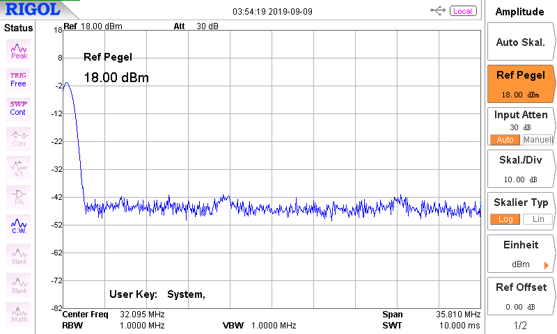
The Transmitter section
The transmitter generally consists of two parts:
- The SSB generator and the TX mixer, and
- the Power Amplifier.
The full schematic of the two parts together:
Microphone amplifier
Starting from the left we see the microphone amp. A nostalgic but still available operational amplifier integrated circuit (741) is used here. The amp has high gain (about 30dB) to make a dynamic microphone connectable. There is no DC feeding for an electret microphone. If you should wish to use one then the negative feedback resistors should be lowered to about 47kΩ and the audio level should be carefully observed to avoid excessive driving. DC must also be applied for htis type of microphone!
Double sideband generator
The MC1496 (still available as NOS in 14 pin DIL case or fresh from the market in SMD package by ON Semiconductors) offers high carrier suppression of about 50 to 60 dB. Therefore a network of 2 x 10kΩ and a 50kΩ variable resistor has been installed. The crucial point: To make full usage of this network the carrier offset must be set properly. If you should notice that there is no point within the full swing of the 50kΩ variable resistor then the carrier frequency should be readjusted.
A balanced output transformer has been installed to improve carrier suppression and to enhance output voltage.
SSB filter coupling out
The usage of shielded cable is mandatory here to avoid transfer of rf stray energy into the DSB and SSB line!
Transmit mixer
This stage also is equipped with an NE612 doubly balanced mixer due to reasons of circuit simplicity.
14MHz Band pass filter
This filter also needs observation. I use the TOKO style coil formers familiar from other projects. The winding data can be found in the schematic. The coil formers must have the ferrite caps and metal shield cans on to avoid incoupling of rf energy from the subsequent power stages. The filter should be placed away from the higher power stages to avoid self-oscillation inside the transmitter section.
RF amplifier power stages
The amplifier presented here has been tested in 2 different radios so far and has proven to be very stable, very linear and very rugged against antenna mismatch. The power levels are about 10 db gain per stage. From the second stage on the output impedance is 50Ω. This makes it easier to measure power levels with a 50Ω standard dummy load.
The 2 watt driver stage uses a PI-filter instead of a broadband transformer. This is because I intended to save some space on the veroboard and for a monoband transmitter this is a practical solution. If you should find out that there is a mismatch that results in losing gain, then the capacitors can slightly be modified because the L-network has impedance transforming capabilities. By knowing input versus output impedance and calculating a “Q”-factor subsequently L and C can be computed to get a defined step-down impedance (Link for further information). This is a useful method and, in case of low pass filter like applied here, there is also a filter for harmonics.
Driver and PA power amp are biased for AB-mode, all other stages operate in A-mode to ensure best linearity. Strategies using emitter degeneration and negative feedback are inherent in preamp and predriver stage.
All transistors apart from preamp stage require usage of heat sinks.
Impedance matching is either not done (stage 1 to 2), by transformer (stage 2 to 3) or by L-network (stage 3 to 4). Whereas from stage 3 to 4 also there is a transformer applied to split the signal symmetrically to the two bases of the final transistors.
If there should be a tendency for self-oscillation within this stage the input transformer secondary winding can be center tapped and put to GND via a 0.1 capacitor.
Power out depends on DC power voltage and is about 20 watts when run on 13.5 V DC power supply an the amplifier terminated to a 50Ω load.
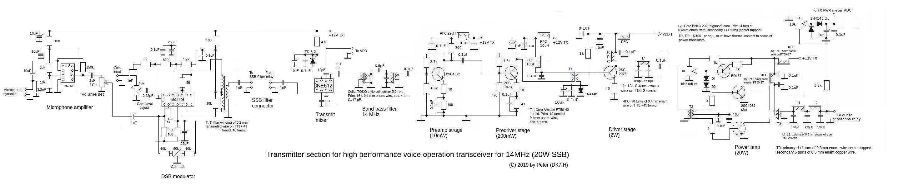
Here
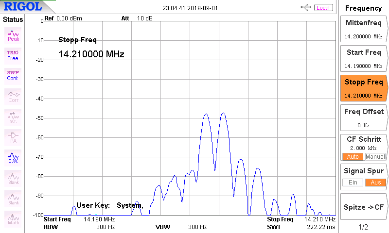
This is a spectroscopical analysis of the fully driven transmitter (f=14.200kHz, Pout = 20.1 watts, VDD=13.0V) and the remaining carrier.
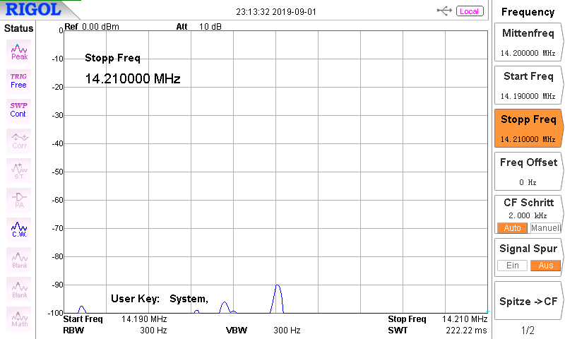
Harmonics are filtered very effectively . This is achieved by using a push-pull final stage driven in AB mode. Some authors say this is useful to eliminate odd number harmonics. On the other hand there are two sections of low pass filtering (one between driver and PA, one following PA). The figure of the output spectrum between and 50 MHz below:
The Dual DDS Oscillator System
The DDS has got the following features:
- VFO: AD9951 + amplifier,
- LO: AD9834 + amplifier,
- MCU: ATMega644P,
- LCD: NOKIA 5110,
- Tuning: Optical rotary encoder by Bourns,
- User interface: 4 keys to control the digital settings,
- Analog inputs: User keys (ADC0), VDD (ADC1), S-Value (ADC2), TX PWR (ADC3), PA Temp. (ADC4).
The schematic:
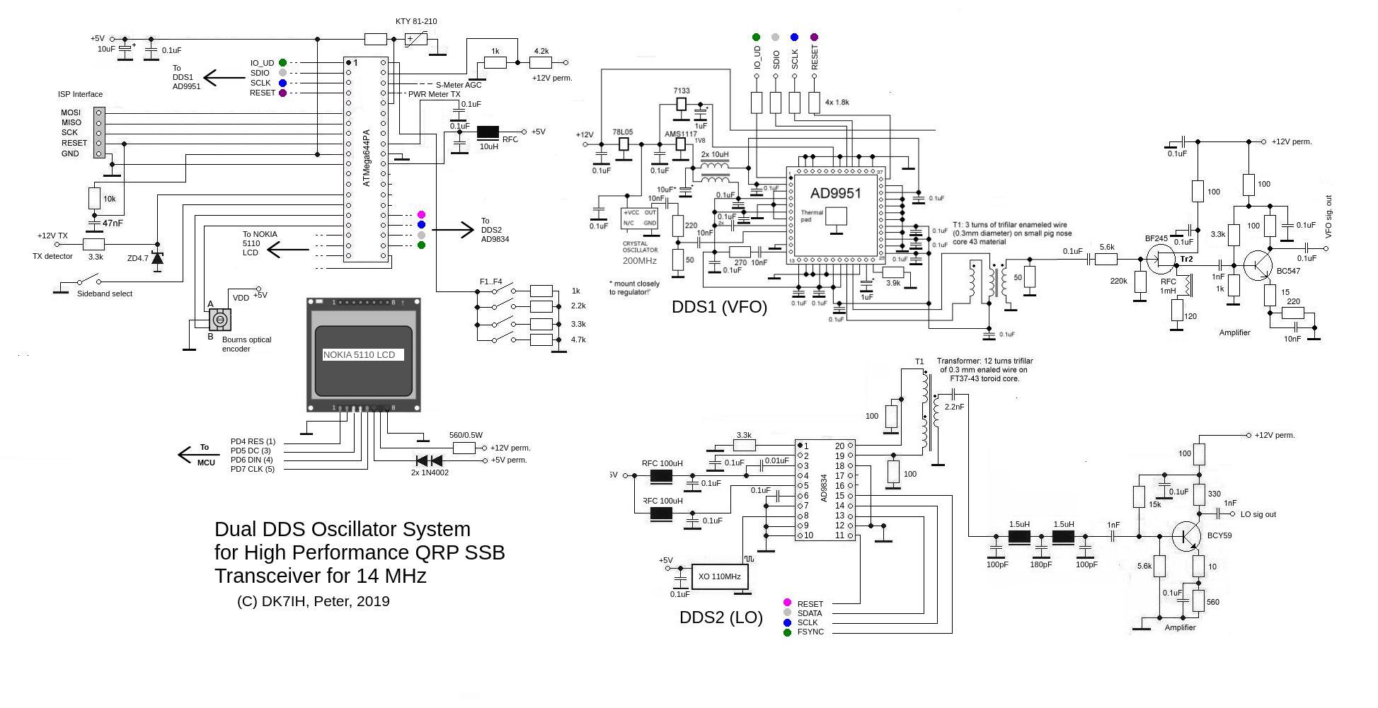
The control lines for DDS1 (AD9951) and DDS2 (Ad9834) are as follows:
//DDS1
//IO_UD: PB0 (1) (green)
//SDIO (DATA): PB1 (2) (white)
//SCLK PB2 (4) (blue)
//RESET PB3 (violet)

//DDS2
//FSYNC: PC0 (1) (green)
//SDIO (DATA): PC1 (2) (white)
//SCLK PC2 (4) (blue)
//RESET PC3 (pink)
The colors are the colors used for the cables in my radio.
The LCD is connected likewise:
//LCD
//RES: PD4
//DC: PD5
//DIN: PD6
//SCLK: PD7
The NOKIA5110 LCD has been designed for VDD=3.3V. Please use 10kΩ resistors in the control lines which are not in the schematic! 3.3V are derived more or less closely by switching 2 Si-Diodes in series which results in a voltage drop of about 1.4V. Hence the LCD gets 3.6V DC from the 5V supply chain which is no problem for the module. One big advantage of the Nokia LCD should not be forgotten: It is very quiet and does not produce any discernable digital noise. Thus it is my favourite meanwhile for receivers on the RF bands.
For both DDS modules coupling out the rf is done with symmetrical circuits using trifilar broadband transformers. 10 turns on a FT37-43 core are a good choice. This will enhance gain and reduce spurs.
DDS2 is clocked to 110MHz, but keep in mind, that AD9834 is specified for 75 MHz max. clock rate only. I found out that modules from the “grey market” sometimes fail and produce lousy signals when overclocked. You can see that on a scope when extra peaks appear or with the spectrum analyzer when spurious signal are frequent. I recommend buying with Mouser or anther trusty vendor for example or reduce clock rate in case of problems in signal quality.
Power consumption is not excessive because both DDS modules are for low power application, unlike the AD9850 or AD9835, that draw much higher current. Power rate is 300mA when in receive mode with LCD backlight on.
The C-code for the software has about 2600 lines source code and can be downloaded here.
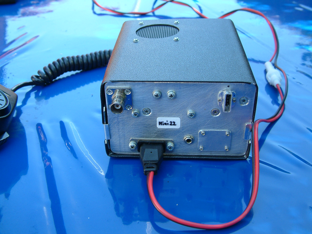
Rear view:
A standard CB DC supply cable is used here. Unfortunatel the plugs equipped with a cable and fuse holder are widely availabe but the sockets have to be stripped from old CB trasnceivers.
On the air the transceiver performs great. Audio is clear and powerful what the QSO partners often tell me. The receiver is fun to listen to, sounding soft AND precise. Maybe I will do a YouTube video the next weeks to prove it! 😉
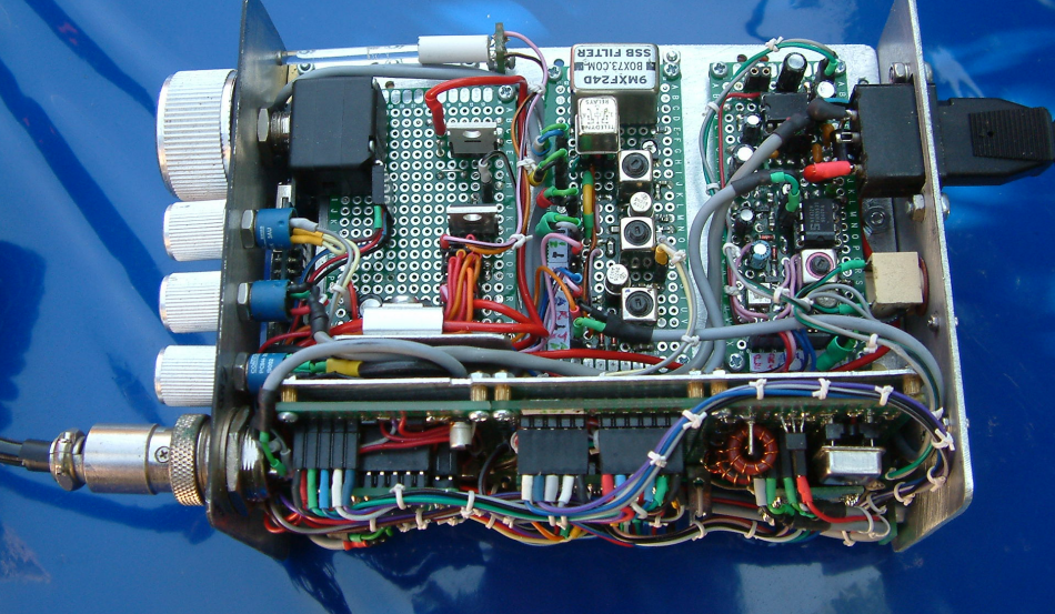
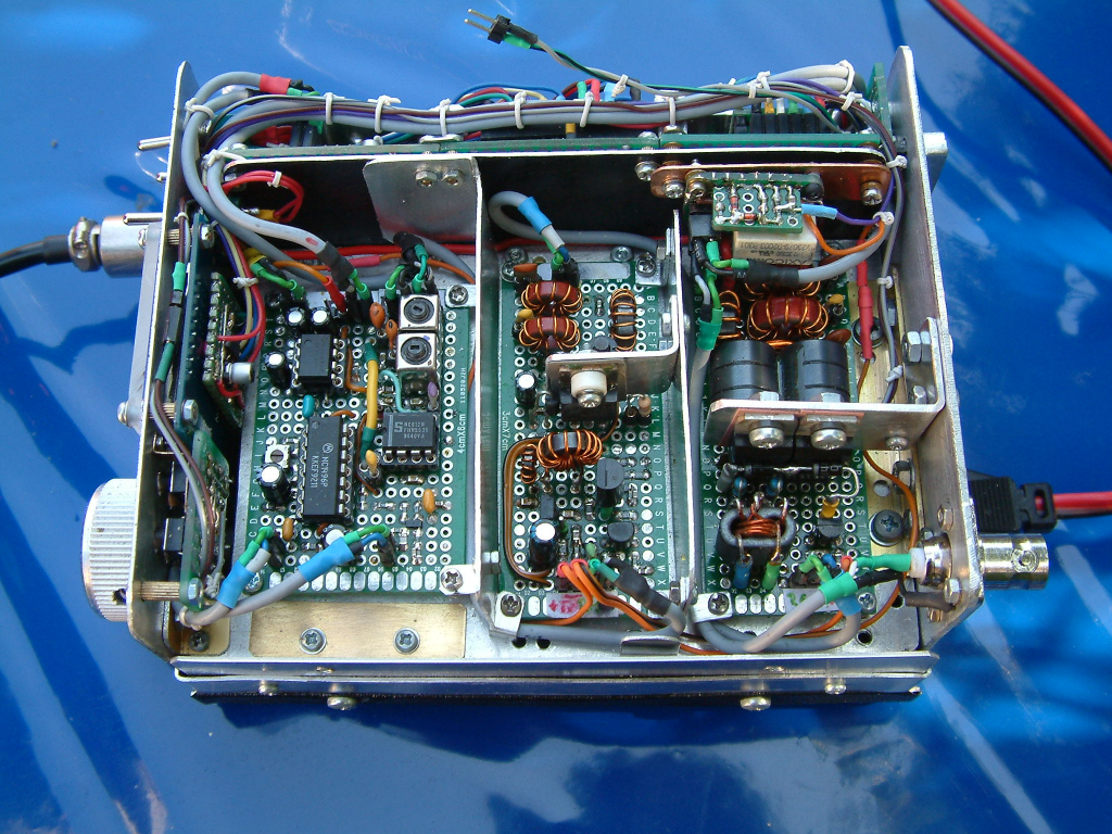
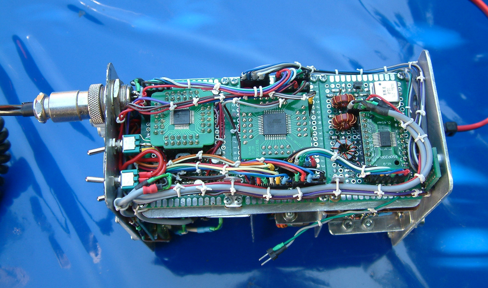
General construction
All my rigs are for portable, hiking, bicycle trips and travel to foreign countries. I use Aluminum as a basis for the hardware to keep the radio lightweight. With this radio a ground plane made of 0.8mm Aluminum sheet metal has been used that one has been enforced with a lateral additional ground plane carrying the DDS system (see pictures in this article, please). Thus the base frame is pretty rigid and not prone for bending.
Front an rear panel are made from 0,.8mm Al sheets (rear) and 0.5 mm Al sheet (front).
The various subassemblies (DDS, receiver, transmitter) are split into different modules and are seperatelay fixed with bolts and washers mounted to special spacer bolts for screws of 2mm diameter. This ensures better grounding instead of using larger veroboards. Connections are made from flexible stranded hook-up wire and shielded cable for rf and audio signals.
On the undersides of the single boards copper foil is used for lines with GND portential.
Vy 73 and thanks for watching! Peter (DK7IH)
Hi Peter, Thanks again for sharing, Good Job!!!
Hi Juan Carlos, thanks a lot and always HAPPY HOMEBREWING! 😉 vy 73 de Peter (DK7IH)
What no filter on the output of the DDS vfo? I see a LPF on the LO (really CO ie: carrier osc). In truth both stages could have broad band pass filters as their range of frequency excursion doesn’t need to be large in a single band rig.
You are an amazing homebrew artist, constantly trying new stuff. I suspect you are tearing down previous projects for parts to build newer ones in the pursuit of perfection (or have the worlds largest junkbox).
Hi there! ;-)) Well, I found out that with such a high clock rate and a comparatively low output frequency a LPF is obsolete. The sine wave is from ideal shape and spectroscopic analysis showed that only the usual harmonics were present but with very low amplitude. I used that DDS at first for experimental purposes and wanted to generate a more or less constant output voltage from 1 to 30 MHz. An LPF would have been interfering with that to a certain degree at least. That is the reason for the fact that LO has got a filter and VFO not.
And, no, I don’t have a large junk box, I do recycling very frequently. 😉 vy 73 de Peter
Thanks For an amazing project and your help with the page. I finally got the page to load. It may be a location issue.
Is it possible to get a copy of the programme code? The link in the article text tells me the page has expired.
I’m looking forward to getting home and building this one.
73, Ian 2W0IWM currently in PY land.