Abstract
When building a direct-digital-synthesis (DDS) frequency generator, the engineer has to take into account one inherit shortcoming of this state-of-the-art technology: Spurious signals that are an unwanted product of generating a radio frequency signal with a synthesizer. These signals occur in a wide range of frequencies and are a limiting factor for receiver performance particularly sensitivity. A method of examining and evaluating these unwanted signal products will be described and some guidelines for amplifier design will be presented.
Introduction
Spurious signals in a DDS system originate from various signal sources in
- the microcontrollers (MCU) driving the DDS. The responsible parts inside the MCU are clock oscillators, dividers, pulse-width-modulation (PWM) timers etc.
- the DDS chip itself mainly from clock dividers and the digital-analog-converters (DACs) used.
Various factors contribute to the problem. First the topology of the synthesizer itself. These systems contain a DAC to form a sine wave signal out of a computer calculated synthesizing data model. DACs have a wide variety of bitwidth. A rule of the thumb is: The more bits the DAC has, the lower the number and the weaker the spurious signals will be. 14-bit DACs by ANALOG DEVICES e. g. perform sufficiently for low noise receivers.
Another topic is clock rate. The occurrence of unwanted signals out of the synthesis process is a reciprocal function of clock rate. So it is highly recommended to use the highest possible clock rate the respective chip is designed for. When experimenting with the AD9951 the following findings occured: From 200MHz primary clock the number of spurious signals significantly decreases. The usage of an internal clock multiplier (if available) is not recommended since it will deteriorate phase noise because another oscillator is added to the signal generating chain..
So far the theory that is common today. Another aspect should now be brought into discussion: The role of the stages that are the successors behind the mere synthesizer. First stage usually is an amplifier that is used to lift the signal level of the synthesizer (usually about 1Vpp.) to a level that it is needed for a certain type of mixer.
The DDS circuit
To eliminate any weakness in the basic generator underlying this research a high-level performance synthesizer has been constructed. This ensures a pure sine wave output which is essential because we want to examine the potentially negative outcomes of the various small signal amplifiers succeeding the synthesizer.
The DDS chip used in this circuit is the AD9951 by Analog Devices that incorporates a 14-bit digital-analog-converter (DAC). Clock rate for the chip here is 200MHz (400MHz max. according to data sheet), clock output is 1.8Vpp. which is the maximum signal level that is suitable for this 1.8V-technology based DDS.
The AD9951 DDS integrated circuit needs 2 supply voltages: 1.8V for the digital and analog circuits and 3.3V for DVDD_I/O, the output driver voltage.
Controls lines are 5V applicable which makes the DDS suitable for being controlled by a 5V microcontroller as well as a 3.3V system.
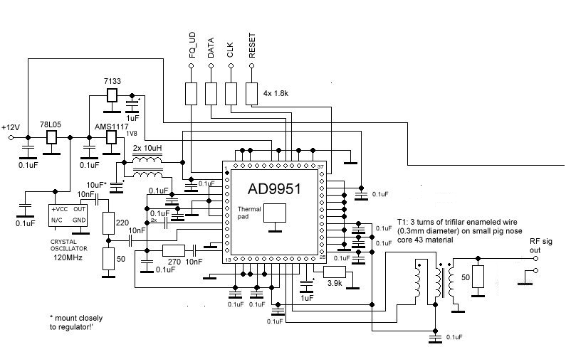
The signal outlet in this case is made from a symmetrical transformer (3 parallel windings 10 turns each on a FT43-37 core) using the IOUT1 and its corresponding paraphase outlet IOUT2. To use the balanced output is another effective possibility to reduce spurious signals as well as to enhance signal voltage by about 3 to 5 dB.
As first step the unamplified signal shall be inspected. In a wider spectroscopic range (f0=8.65MHz, fgen.=16MHz, f1=250.0MHz) the signal performs as shown below where f0 and f1 are the edge frequencies of the spectrum analyzer and fgen. is the output frequency of the DDS):
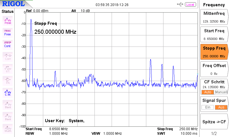
A first spurious signal can be detected with a signal level of more than 40dB below the generated signal. The signals at around 100MHz supposedly are strong FM stations in the VHF radio band whose energy from a nearby radio tower is coupled into the laboratory via the short wave antenna cable ending on top of the workbench. The peaks around 200 MHz are likely generated by the DDS clock oscillator.
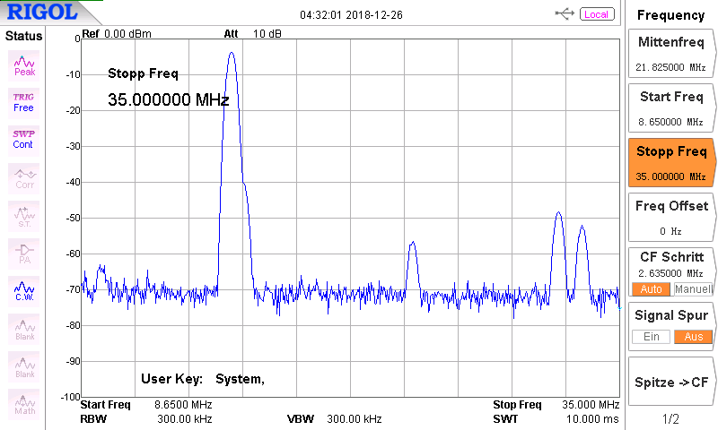
Switching to a more narrow spectrum, we get this reading:
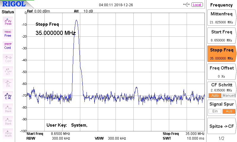
Remarkable that there is no even first harmonic that should be expected around the 32 MHz region. It is highly probable that this elimination of the 1st harmonic is caused by the symmetrical decoupling of the signal from the DDS. Hence we know that push-pull operated amplifiers reduce distortion and therefore tend to minimize even harmonics production.
Remarkable on the right falling edge of the main peak there another signal occurs hidden by the main curve which requires further examination.
Examining amplifiers for a DDS system
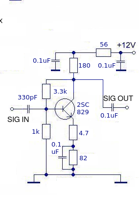
1.) Bipolar RF preamplifier circuit (adapted from DeMaw et. al., Solid state design for the Radio Amateur)
The first amplifier under test is a simple circuit containing a bipolar transistor. To reduce distortion emitter degeneration and negative feedback (from collector to base) have been installed. This is an amplifier that is often used in rf amplifiers as first stage of the power strip. Therefore it should contribute less to the overall distortion of the circuit.
Overall voltage gain with a 2SC829 RF transistor (fT=230MHz) is 13dB with 1 MHz, decreasing about 3 db per octave, power gain has not been evaluated.
With the settings of the spectrum analyzer unchanged it turns out that this amplifier obviously produces new signals that are prone to disturb the receiver of a radio where this amplifier is installed:
Signal level is about 2V pp.
One countermeasure is to carefully check the input level of the amplifier. Excessive input voltage will bring the amplifier into the clipping area thus generating IMD products and harmonics. We usually do not only observe the output signal with an oscilloscope but use the spectrum analyzer in parallel. This ensures optimized signal quality.
Proper biassing is essential for this type of amplifier, aside from the linearization described before. The operating point (also referred to as “Q-point) must be set in the middle of the linear part of the IBE->IC function.
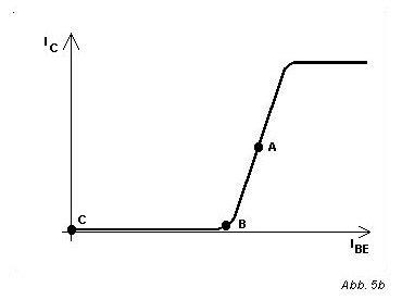
Usually this is achieved by applying a positive voltage (for NPN transistor) so that a given “quiescent” current flow through the base-emitter line. In the most simple case a voltage divider with the base connected to the joint of the two resistors works satisfactory.
Any AC voltage applied now will alter the voltage sum of DC (quiescent) and AC around the Q-point.
Vres.= VDC+VAC
whereas VAC=V0*sin(ωt)
(To be continued)
by Peter, DK7IH
Hallo Peter
Wir haben uns am SWT gesehen.
Ich habe deine AD9951 Schaltung als Vorlage genommen und ein Layout gezeichnet.
Ich will dir die Schaltung zeigen. Kannst du bitte einen Blick darauf werfen? Ob das soweit richtig ist.
Ich sende dir die Schaltung via Mail zu.
73 Heinz HB9KOC
Hallo Heinz,
ja, das kannst Du gerne tun. Allerdings komme ich erst übernächste Woche dazu, denn da habe ich Herbstferien.
Vy 73 de Peter