The two DDS oscillators are mounted to the side of the cabinet. They are sited close to the microcontroller board to keep leads short.
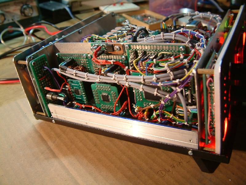
Right on the left you can see the small dual-tone oscillator for testing and tuning. Next is the AD9834-equipped local oscillator (LO), centered the AD9951 that serves as the VFO. Right the ATmega128, mounted to a 64 lead breakout board can bee spotted behind the varios cables going to and from this section.
The Dual-Tone Oscillator
This one consists of two simple phase-shift audio oscillators. I have introduced this circuit a longer time ago for testing purposes here in this blog.
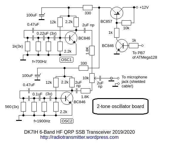
The capacitors and resistors in the phase-shifting chain have been chosen to put the two different frequencies to values of about 700Hz and 1900Hz, thus they are not harmonically related. A variable resistors allows the user to set the balance between the two signals so that they are equal in voltage.
Two transistors (a PNP-NPN pair) are switched by Pin PB7 from the microcontroller. There is a respective function in the software that activates the transmitter together with this oscillator for comfortable tuning and testing.
The Local Oscillator (LO)
This one again uses the “good old” AD9834, overclocked to 100MHz. I found that some chips from the “grey market” have problems when being overclocked and therefore produce spurious signals. In case this occurs, it is recommended to step back to the clock frequency of 75 MHz which is high enough for the purpose of the LO.
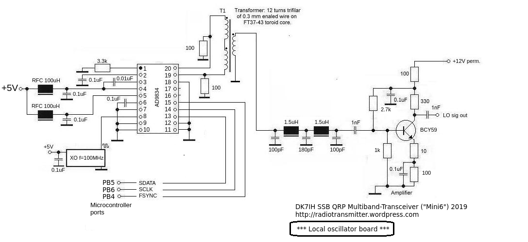
The oscillator comes with an balun output transformer (will reduce spurs!) and a low-pass filter plus a simple amplifier. The latter basically is not necessary because the LO will only have to drive the inputs of SA602 integrated mixer circuits (200mV RMS) used as SSB generator and rx demodulator. I had another mixer type in mind before, that one needed higher voltage. Thus the coupling to PIN6 of SA602 is only via 5.6pF capacitor to avoid overdriving the mixer and improve signal purity. This will be shown later when we are about to discuss receiver and transmitter circuitry.
The VFO
Here the AD9951 DDS again comes to operation. This one has got a 14-bit DAC which makes it less prone for spurious signals. The clock rate has been pushed to the limit of 400MHz which, according to datasheet, is the max. clock rate for this DDS module.
You can download a datasheet of a suitable clock oscillator. This device is very small but it can be soldered to a 2 by 2 hole piece of veroboard and then mounted to a piece of headerstrip by soldering wires to the underside of the board:
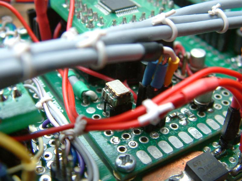
A voltage divider will reduce the 3.3 V to 1.7V that is acceptable for the clock input of the AD9951 chip.
The DDS circuit is common for frequent readers of this blog:
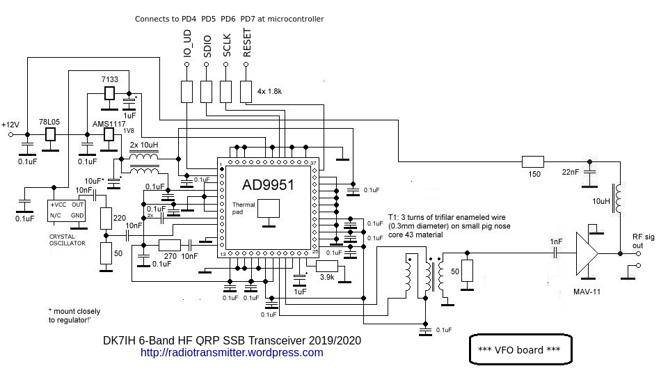
The low pass filter has been left out because when examining the output signal of the DDS it turned out to contain only very little quantum of harmonics. The max. frequency of this VFO will be 29.7 MHz + 9MHz which equals to 38,7 MHz.
Thanks for reading and stay tuned! 😉
Peter (DK7IH)
I disagree with not including a simple LPF for the DDS. Even though the clock frequency is over 10 times the desired output, it’s still possible that unwanted spurs might find their way into the desired output. A simple LPF with a corner frequency of 40mhz would be good piece of mind, and would only need 5 passive parts.
Hi there, OK, but first I have checked the spectrum of the DDS output with a spectrum analyzer and could not find spurs. And second, ih there were spurs, they would pass the LPF and occur in the receiver chain. And for the transmitter there are BPFs so that no unwanted signal can be amplified out of the passband. Vy 73 de Peter
Peter, your sense of scale is almost an order of magnitude smaller than mine, and nearly every other maker of superhet transceivers I’ve seen. I say this because you describe this rig as ‘experimental, and that it has space and a layout to allow board replacement and repair. To me it looks beautifully compact. Let’s see how this story continues… VK3HN.
How did you manage to ground the underneath of the chip – my board looks very similar to yours, but no central pad
Hello Nigel,
I have not soldered the “pad”to GND. It works anyway but I can’t compare with the soldered version. vy 73 de Peter
Hi Peter,
Thanks for your swift reply.
I was going to mill a hole in the back of the PCB!
Heck I’ll try it anyway.
I’ve had the chip in my box for about 4 years.
73
Nigel