This unit basically consists of two parts:
- SSB-Generator and TX-mixer
- TX-power amplifier stages
The SSB-Generator and TX-Mixer Board
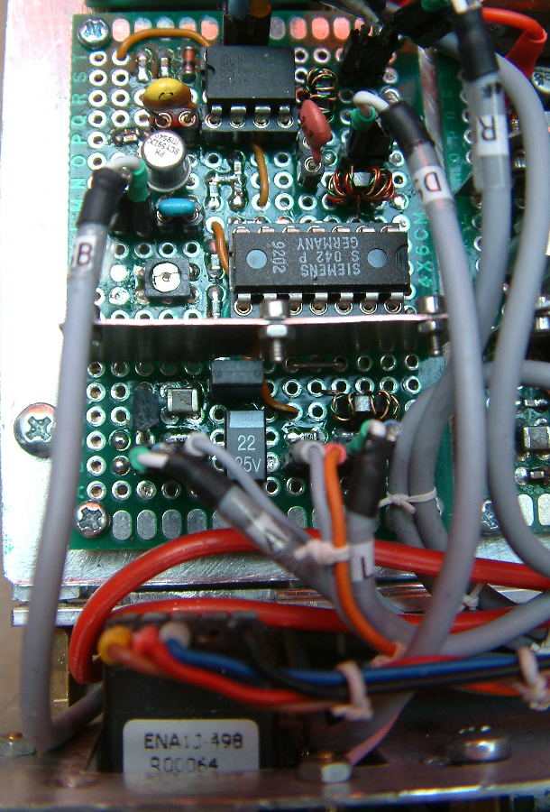
After having built this respective board with two NE612 ICs (one for DSB generator, one for the TX mixer) I was not satisfied with carrier suppression of the DSB generator. It turned out as only 40dB. Afterwards I constructed a new board with an old SIEMENS Mixer IC (S 042 P) that is still available NOS from various sources. With this one I gained carrier suppression rates of around 55dB. I think this is OK for a homemade transceiver.
The board looks as follows, set up on a 6x4cm 0.1″ veroboard:
The circuit starts with an AF amplifier equipped with a bipolar transistor where also a power supply for Electret microphones has been added. The radio now can handle dynamic and Electret microphones adequately.
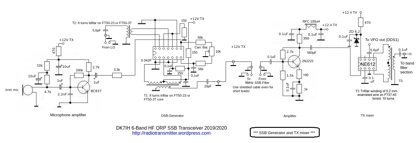
Afterwards we see the S042P mixer IC where I have changed the circuit slighty to the one used in my 40-meter-QRO TRX. Audio input signal is now to PIN8 of the IC, Lo input on the rf side of the IC to PIN11 and PIN13. To reduce carrier level and enhance carrier suppression a 5.6pF cap is in series because the relatively high level of signal coming from the LO amp would deteriorate the performance of the DSB generator without countermeasures.
Output from this DSB generator is also symmetric and fairly high. Thus a low valued capacitor has been inserted prior to the SSB filter, sited on the RX board.
After that we see an amplifier with limited gain due to high emitter degeneration and the NE612 as TX mixer. The latter one also with an symmetric output to get more gain from it by using the two inherent output transistors.
TX-power amplifier stages
As I have described in the article of my “Give me 5“-Transceiver some years ago, building a broadband power amplifier is challenging due to one special problem related with the wide range of frequencies that this amplifier must be able to cope with. an extra gain of 5 to 6 dB is commen, when the frequency is divided by the factor of 2. Usually the necessary compensation is done by adding adequate capacitors and inductances using their frequency depending reactance.
With this radio I tried something new. I added an amplifier that is gain controlled by an adjustable voltage. Here a dual-gate MOSFET with gain control to gate 2 sets up the initial stage of the whole amplifier strip. The stage’s gain is set by a simple bipolar driver transistor controlled by a digital-analog-converter (DAC). A numeric value for each individual band is stored with in the EEPROM of the MUC. This numeric value is calculated during adjustment, then stored in the MUC and recalled whenever the radio is switched to a certain band. The DAC is an MCP4725 breakout board, containing a 12-bit device.

After that we see an amplifier that is common solid state technology. Preamp stage and predriver stage are set to A mode which requires a heat sink for the predriver stage. Here a 2N3866 is used as amplifying element.
Driver stage is single ended, operates in AB-mode and also is protected by a heat sink.
After that a somehow uncommon technique has been applied. Instead of using a broadband transformer to reduce the stages output impedance to the some ohms input impedance of the final stage, a set of 6 switchable low-pass-filters is used.
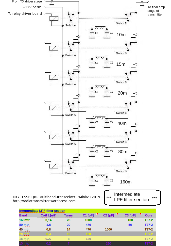
This filter section has been optimized to an output impedance of 50 ohms for each band thus enabling me to test and optimize the transmitter to a maximum with a defined output impedance (remember, this is an experimental radio! 😉 ).
After this filter section the final amplifier stage follows which is able to drive the output power up to 15 to 20 watts on all bands but depending on the DC voltage used for transmitting. The max. power gained during tests was 22 watts pep at 15V DC with two NTE236 transistors. Unfortunately the turned out not to be so rugged and blew in the tests. The eleflow 2SC1969 inserted later showed no problems at all. Thank God! When running on 12.0 V DC the amplifier puts out 12 watts at all bands.
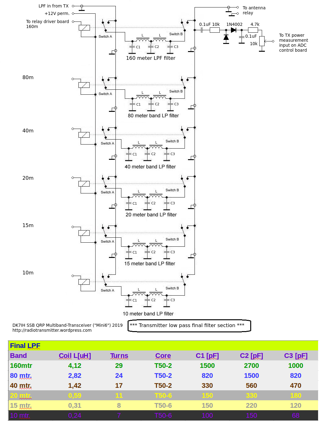
The final part of the transmitter section is the last low-pass filter that is positioned next to antenna relay in the same compartment:
The whole transmitter looks like this:
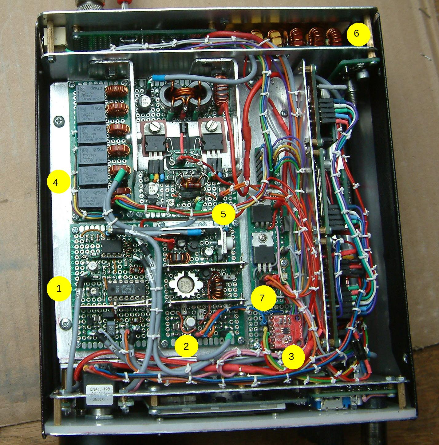
The various units are:
- 1: DSB-Generator and TX mixer
- 2: Amplifier stages 1 to 4
- 3: MCP4725 transmitter gain controller
- 4: Intermediate LPF board
- 5: Power amplifier
- 6: Final LPF section
- 7: TX/RX switch board
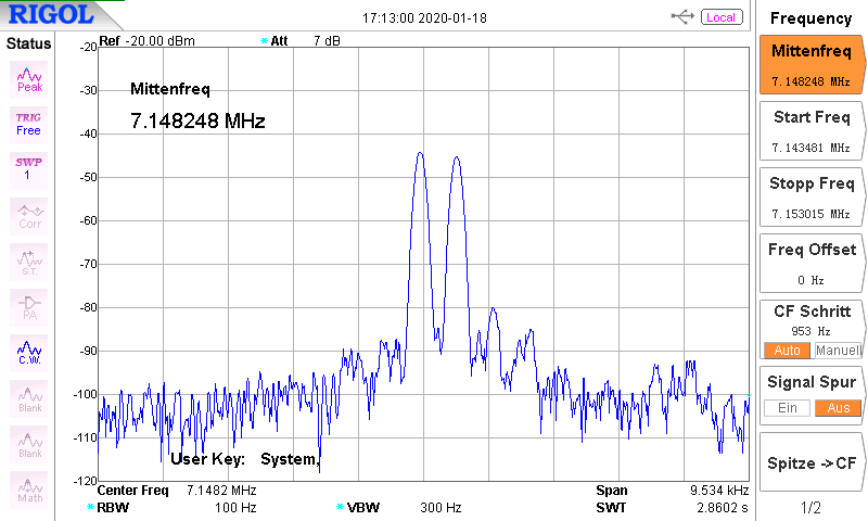
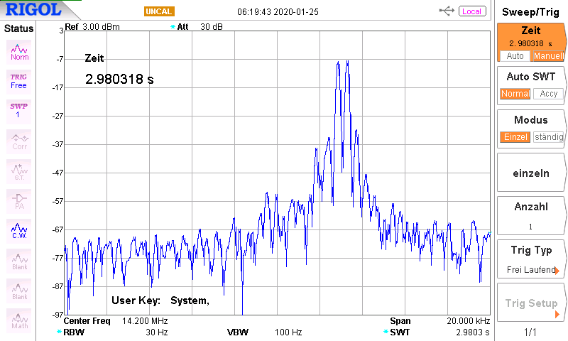
Here a little bit of analysis to end with the article. First is the output of the SSB-Generator/TX-mixer board with maximum output (Around 500mV pp) set to the 40m band.
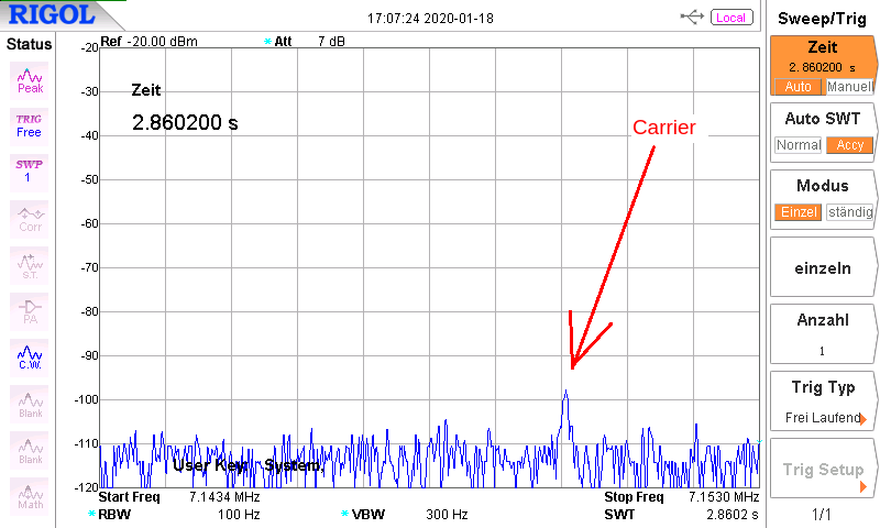
Nest we see the carrier suppression when dual tone audio in has been suspended. Carrier is about 55db under the signal peak.
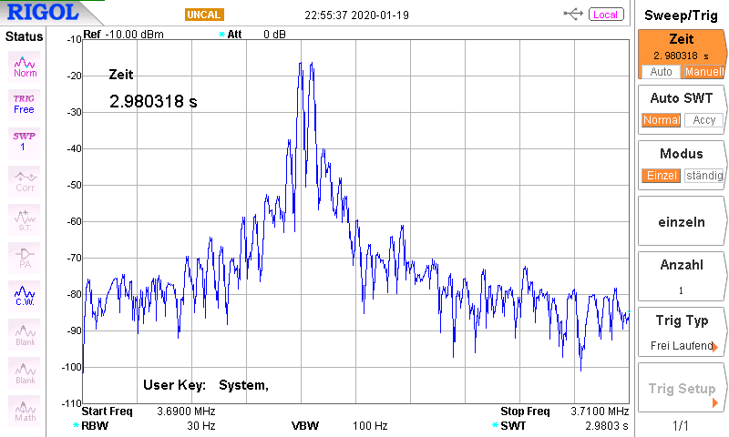
And here an output signal with max. power at 3.5 and 7 MHz:
So, that’s all for today, thanks for watching and 73!
Peter (DK7IH)
I would suspect that the MC1496 balanced mixer would give similar performance to the SP042. This part is still being made by ON-Semiconductor.
Well, I think you are absolutely right. But the number of parts needed for the MC1496 is much higher than the quantity for the S042P.
vy 73 de Peter
Not really, IIRC. Perhaps a few extra biasing resistors and bypass caps. However I suspect that the Siemens parts are more readily available on your side of the pond. I’m interested in building a rig similar to this one, but I might make use of the Hybrid Cascode circuit from QST for the IF and RF circuits along with its IF derived AGC rather than your audio derived circuit. I have several identical 9mhz IF filters, so I might use one in the RX and another in the TX side, thereby eliminating one switching relay. I also might try using the SI5351 instead of both DDS circuits. While the DDS units might have better phase noise figure on paper, given the good results others have had with this circuit, I suspect the difference will be hard to determine without expensive test equipment.
Please post more detailed construction photos, while I might not follow your exact design, I would like to see how you manage to cram all that good stuff into a small space. I would also like to see how you build those neat enclosures!
You have made a very nice transceiver here and documented it extremely well! I have been building similar projects since 1980 and enjoy seeing other’s approach to the same design and packaging problems. See some of my projects at http://wa3tfs.com.
73, Jim
Hi Jim, thanks for the compliments. Just openend your website. Looks really great, so I have bookmarked it for later visit. Thanks a lot! Vy 73 de Peter
Nice Peter… I think i will do that too… I already ordered all components for Rx. 73 de 9a3xz Mikele
Peter, a superb piece of radio craft again. I am still in awe of the neatness and density of your rigs. I just dont find the patience that you find for precise cabling, looming, heatshrink cover, labelling, to name a few things. Once again, well done!
All my multiband receiver and transceiver projects suffer from gain drop off above 10MHz. I have resorted to using a switched preamp in the Rx. I’d thought of your idea of using a D to A block to gain control a preamp stage and you’ve showed us how. And the D-A is an eBay breakout. I might get a few.
I think you could just run the DG MOSFET gate 2 direct from the D-A as most of the gain range is in the 0.5 to 3V range.
73 Paul VK3HN
Hi Paul, I think from the interior my radios look more or less like the CB-transceivers from the 80s. 😉
Currently I am optimizing the MUC controlled gain setting for the transmitter and will report the following weekend. An the also the mechanical parts will be discussed because scharkalvin has asked concerning this topic.
vy 73 de Peter (DK7IH)
Peter ,only for info…this rtx i built before one year but for 80m band.This project also you can find many many projects from big dr.Matijaz Vidmar s53mv from Slovenia about SO42P from 1985. 😉 😉
http://lea.hamradio.si/~s53mv/archive/a015.pdf
Thanks very much for the link. I don’t understand the language but I can read schematics! 😉 Great old piece art! 73 de Peter (DK7IH)