Abstract
This uni of our online tutorial will cover the implementation, configuration and usage of I2C communication with the STM32F4 MCUs. Later we will show practical examples, that can be used for driving an SH1106 OLED display for example or a 24C65 external EEPROM.
I2C basics
I2C (spoken “I square C” for inter-integrated circuit) has been developed by Philips Company in the beginning of the 1980s. It is a two-wire serial bus system with one master and one or multiple slaves connected to a common bus. With ATMEL this is called TWI (“two wire interface” due to copyright reasons).
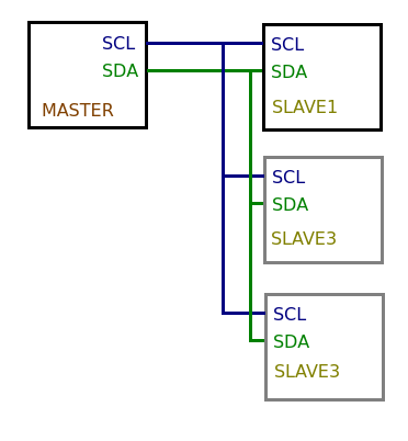
SCL (Serial Clock) is a permanent clock signal and SDA (Serial DAta) is the data line. Each slave is identified by a unique 7-bit address. Thius often is coded as
uint8_t device_addr = 0x78; //I2C_DEVICE_ADDRESS; here for OLED SH1106
The remaining bit (LSBit) indicates to the slave either the it should receive data from or transmit data to the master.
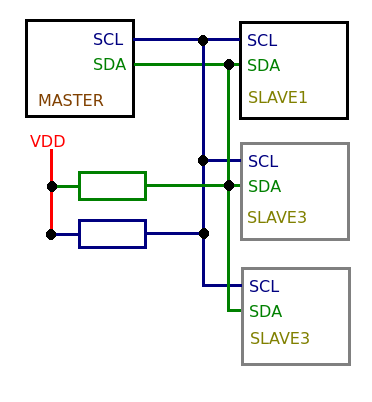
In practical circuits it is important that the two lines (SCL and SDA) must be pulled up with resistors (2.7 to 4.7 kOhms) to VDD to make sure that the ports of the ICs used for master and slave can pull down the lines when data or clock is transmitted. This system generates the mandatory voltage swing between 0V and VDD on the 2 lines.
I2C on STM32F4
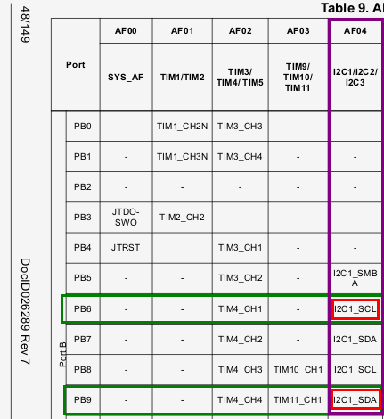
I2C uses ports by applying “alternate function” mode (AF) to the respective pins. In this demonstration we will use ports B6 as SCL and B9 as SDA.
First we have to enable the related clock for I2C communication:
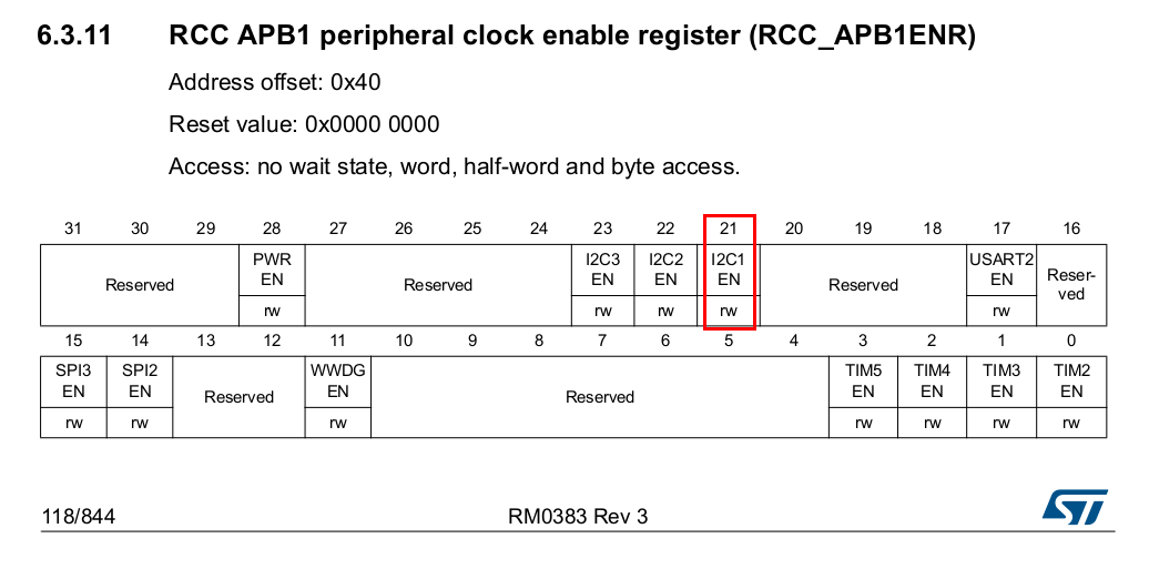
As we want to activate I2C interface 1 (I2C1) we have to set high the corresponding clock by setting bit 21 as “1”:
RCC->APB1ENR |= (1 << 21);
The following sequence does the port definition as alternate function with open drain output (we are about to use pull up resistors, please remember!)
//Setup I2C PB6 and PB9 pins
RCC->AHB1ENR |= (1 << 1);
GPIOB->MODER &= ~(3 << (6 << 1)); //PB6 as SCK
GPIOB->MODER |= (2 << (6 << 1)); //Alternate function
GPIOB->OTYPER |= (1 << 6); //open-drain
GPIOB->MODER &= ~(3 << (9 << 1)); //PB9 as SDA
GPIOB->MODER |= (2 << (9 << 1)); //Alternate function
GPIOB->OTYPER |= (1 << 9); //open-drain
Based on the table above and having prepared PB6 and PB9 for AF use we have to program AF4 (0b0100) for PB6 in AFRL (aka AFR[0] in CMSIS) and PB9 in AFRH (aka AFR[1] in CMSIS):
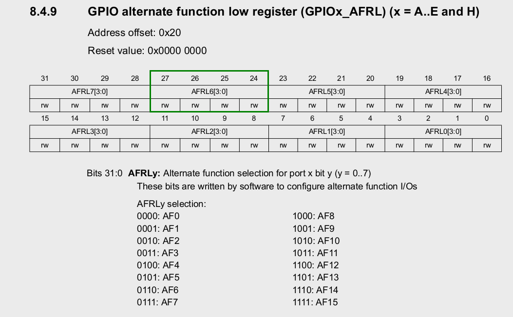
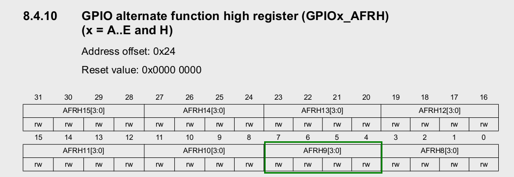
//Choose AF4 for I2C1 in Alternate Function registers
GPIOB->AFR[0] |= (4 << (6 << 2)); // for PB6 SCK
GPIOB->AFR[1] |= (4 << ((9-8) << 2)); // for PB9 SDA
The next steps perform a software reset of the register and subsequently reset this I2C configuration register:
//Reset and clear register
I2C1->CR1 = I2C_CR1_SWRST;
I2C1->CR1 = 0;
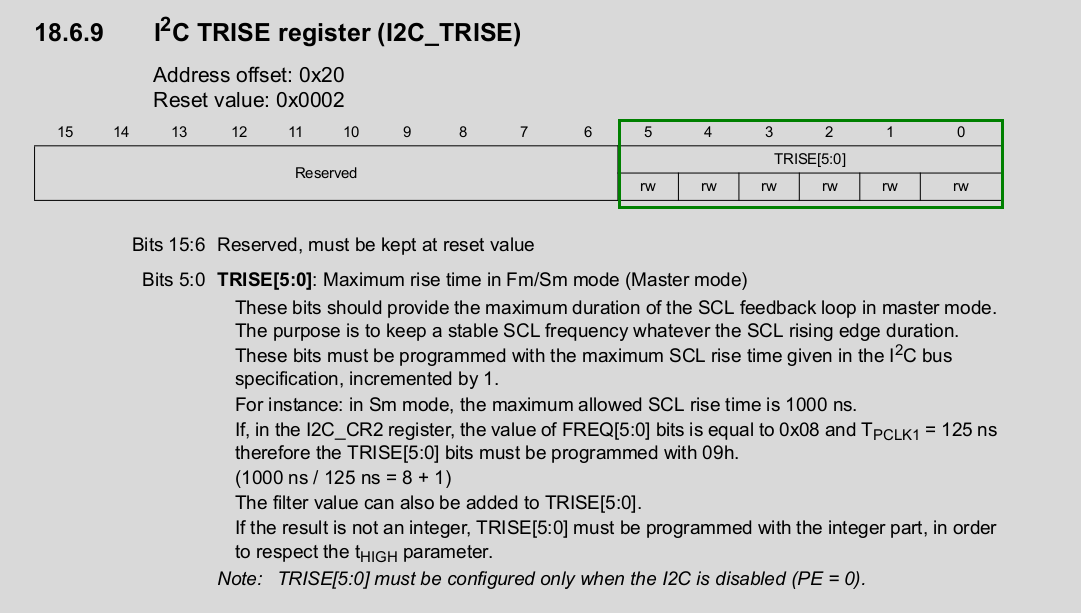
The last steps are defining the clock frequency for the I2C bus based on APB hub frequency and enabling I2C interface:
//Set I2C clock
I2C1->CR2 |= (10 << 0); //10Mhz peripheral clock
I2C1->CCR |= (50 << 0);
I2C1->TRISE |= (11 << 0); //Set TRISE to 11 eq. 100khz
I2C1->CR1 |= I2C_CR1_PE; //Enable i2c
//I2C init procedure accomplished.
As you can see from CR2 register description that peripheral is defined in I2C->CR2 register (bits 5:0) and bits 11:0 in CCR register. It is strongly recommended to take a view in the reference manual chapters 18.6.2 (CR2 register) and 18.6.8 (CCR register). The same is valid for TRISE definition:
Sending and receiving data via I2C
Sending 1 byte of data
Before we define the a function for sending 1 byte of data we may look like first to 2 functions to be defined to start and stop an I2C data transfer:
void i2c_start(void)
{
    I2C1->CR1 |= (1 << 8);
    while(!(I2C1->SR1 & (1 << 0)));
}

void i2c_stop(void)
{
    I2C1->CR1 |= (1 << 9);
    while(!(I2C1->SR2 & I2C_SR2_BUSY));
}
Next we program the transmit function:
void i2c_write_1byte(uint8_t regaddr, uint8_t data)
{
    //Start signal
    i2c_start();

    //Send chipaddr to be targeted
    I2C1->DR = DeviceAddr;
    while (!(I2C1->SR1 & I2C_SR1_ADDR)); //Wait until transfer done
    //Perform one read to clear flags etc.
    (void)I2C1->SR2; //Clear address register

    //Send operation type/register
    I2C1->DR = regaddr;
    while (!(I2C1->SR1 & I2C_SR1_BTF)); //Wait until transfer done

    //Send data
    I2C1->DR = data;
    while (!(I2C1->SR1 & I2C_SR1_BTF)); //Wait until transfer done

    //Send stop signal
    i2c_stop();
}
When we wish to write more than one byte we have to hand over a pointer to the data we want to transmit as well as the number ob bytes to be transmitted:
//Multiple number of bytes (2+)
void i2c_write_nbytes(uint8_t *data, uint8_t n)
{
    int t1 = 0;

    //Send start signal
    i2c_start();

    //Send device address
    I2C1->DR = device_addr;
    while (!(I2C1->SR1 & I2C_SR1_ADDR));
    //Perform one dummy read to clear flags
    (void)I2C1->SR2;

    for(t1 = 0; t1 < n; t1++)
    {
        //Send data
        I2C1->DR = data[t1];
        while (!(I2C1->SR1 & I2C_SR1_BTF));
    }

    //Send stop signal
    i2c_stop();
}
And if you wish to receive data from the I2C system, here 2 examples how to do this. The 1st one calls a one-byte address and returns the 8 bit value for register, the 2nd one can address a word register (16 bits) an return the containing byte for example in EEPROMs like the 24C65 IC.
//Address a byte register, return one byte
uint8_t i2c_read1(uint8_t regaddr)
{
    uint8_t reg;

    //Start communication
    i2c_start();

    //Send device address
    I2C1->DR = DeviceAddr;
    while (!(I2C1->SR1 & I2C_SR1_ADDR));
    //Dummy read to clear flags
    (void)I2C1->SR2; //Clear addr register

    //Send operation type/register
    I2C1->DR = regaddr;
    while (!(I2C1->SR1 & I2C_SR1_BTF));

    //Restart by sending stop & start sig
    i2c_stop();
    i2c_start();

    //Do it again!
    I2C1->DR = DeviceAddr | 0x01; // read
    while (!(I2C1->SR1 & I2C_SR1_ADDR));
    (void)I2C1->SR2; //Dummy read

    //Wait until data arrived in receive buffer
    while (!(I2C1->SR1 & I2C_SR1_RXNE));
    //Read value
    reg = (uint8_t)I2C1->DR;

    //Send stop signal
    i2c_stop();

    return reg;
}

//Address a word register, return one byte
uint8_t i2c_read2(uint16_t regaddr)
{
    int8_t reg;
    int16_t r_msb, r_lsb;

    r_msb = (regaddr & 0xFF00) >> 8;
    r_lsb = regaddr & 0x00FF;

    //Start communication
    i2c_start();

    //Send device address
    I2C1->DR = device_addr;
    while (!(I2C1->SR1 & I2C_SR1_ADDR));
    //Dummy read to clear flags
    (void)I2C1->SR2; //Clear addr register

    //Send operation type/register MSB
    I2C1->DR = r_msb;
    while (!(I2C1->SR1 & I2C_SR1_BTF));

    //Send operation type/register LSB
    I2C1->DR = r_lsb;
    while (!(I2C1->SR1 & I2C_SR1_BTF));

    //Restart by sending stop & start sig
    i2c_stop();
    i2c_start();

    //Repeat
    I2C1->DR = device_addr | 0x01; // read
    while (!(I2C1->SR1 & I2C_SR1_ADDR));
    (void)I2C1->SR2;

    //Wait until data arrived in receive buffer
    while (!(I2C1->SR1 & I2C_SR1_RXNE));
    //Read value
    reg = I2C1->DR;

    //Send stop signal
    i2c_stop();

    return reg;
}
Full code example can be downloaded here.
What can be seen as a useful homework: Reprogram the functions in a way that you can write one byte to a word register for EEPROMs like 24C65.
Thanks and hope to see u again!
vy 73 de Peter (DK7IH)