Abstract
This article describes a QRP transceiver for the 10 HF bands (160, 80, 60, 40, 30, 20, 17, 15, 12 and 10m) exclusively for SSB. Strictly speaking, the 30m band would be superfluous, but since the digital logic that I use to switch the band relays has 10 outputs, I added the 10-MHz band. This is, admittedly, just for listening purposes.
The transceiver uses the single-interfrequency model, in this case 9MHz are applied. The main features of this radio given as a survey:
- It’s a “Hardware defined radio”,
- Bands are 160, 80, 60, 40, 30, 20, 17, 15, 12 and 10m,
- Transceiver control uses a microcontroller (STM32F411) with about approx. 1800 lines of source code written in C,
- VFO is a DDS with an AD9951 (frequency is always above the IF),
- The local oscillator LO is a Colpitts circuit,
- The radio contains one set of band filters (10 * 2 LC-circuits ), used alternately for TX and RX.
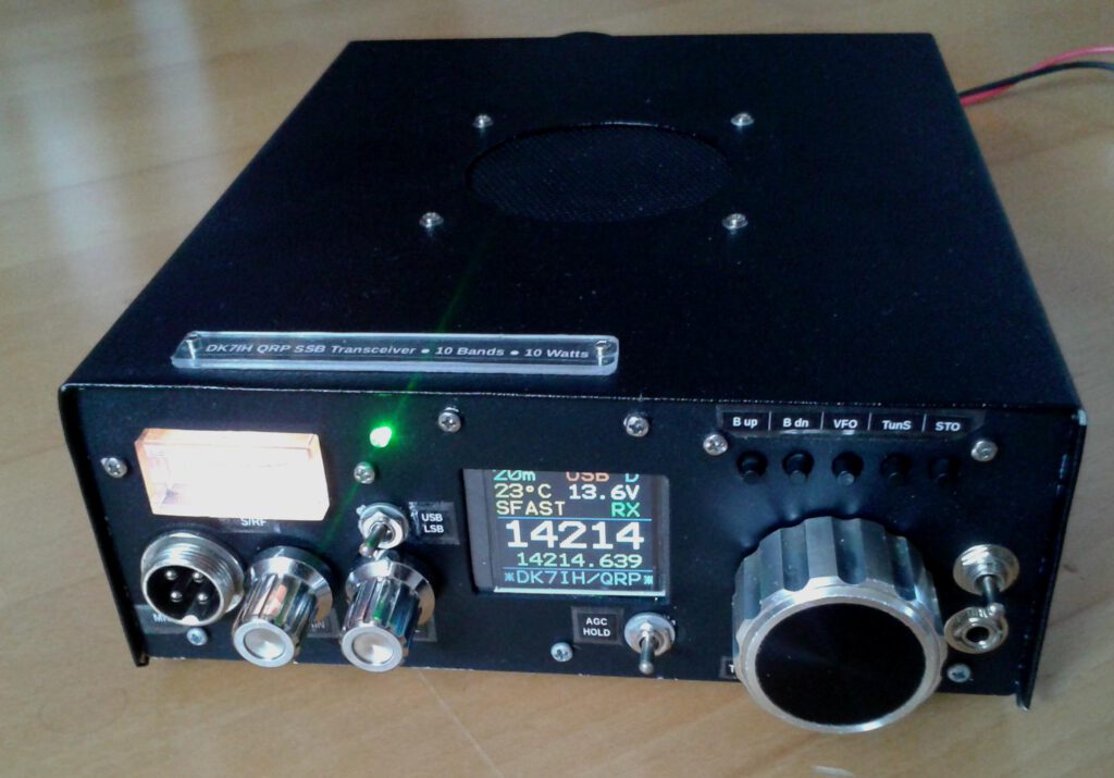
Mechanical construction: The radio is built with 2 levels with hinged top level (RX and MCU above, TX below) Dimensions: (width * depth * height) 16*18*6cm
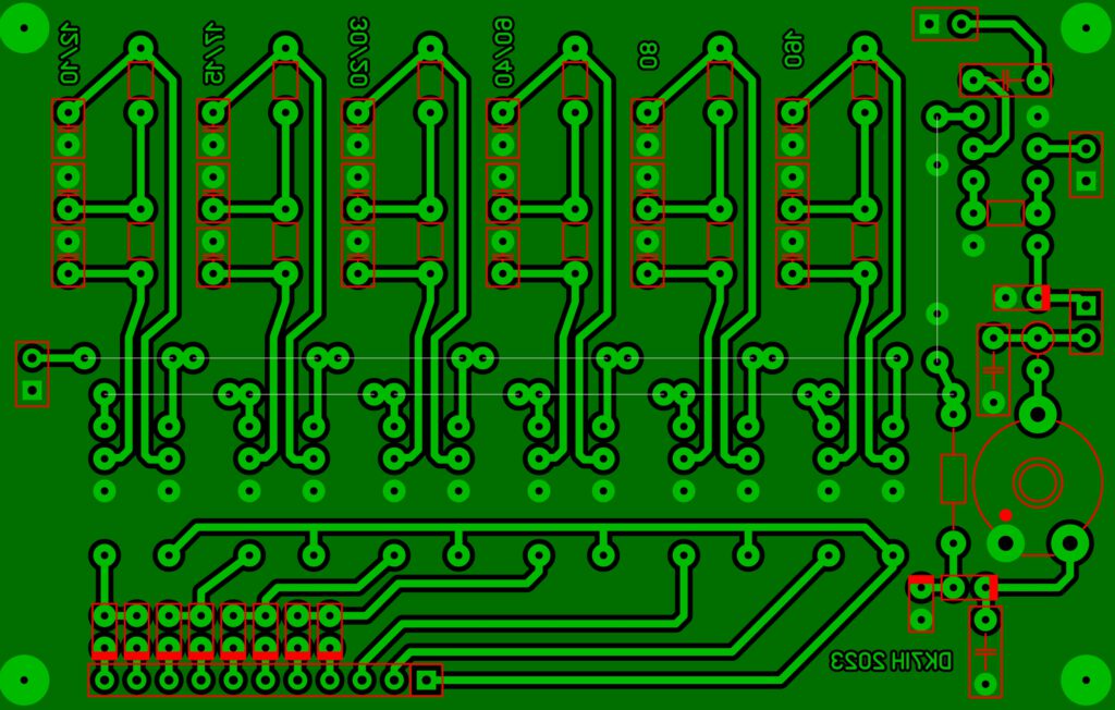
The whole electronic circuit consists of on 13 separate PCBs due to the possibility for optimization of the radio.
Inside the radio – Details on construction
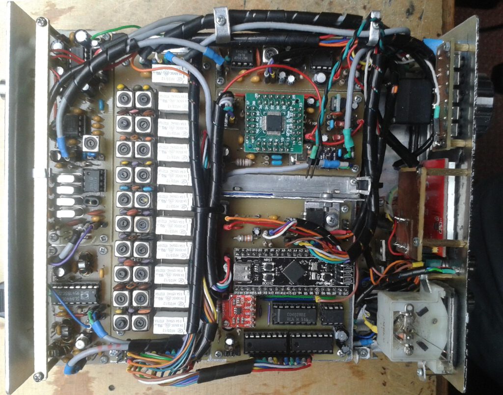
As already mentioned the radio consists of two compartements. The upper one consists of the microcontroller unit, the DDS (both on the right side of the picture), the AGC circuit, the bandfilter section and the receiver unit (on the left):
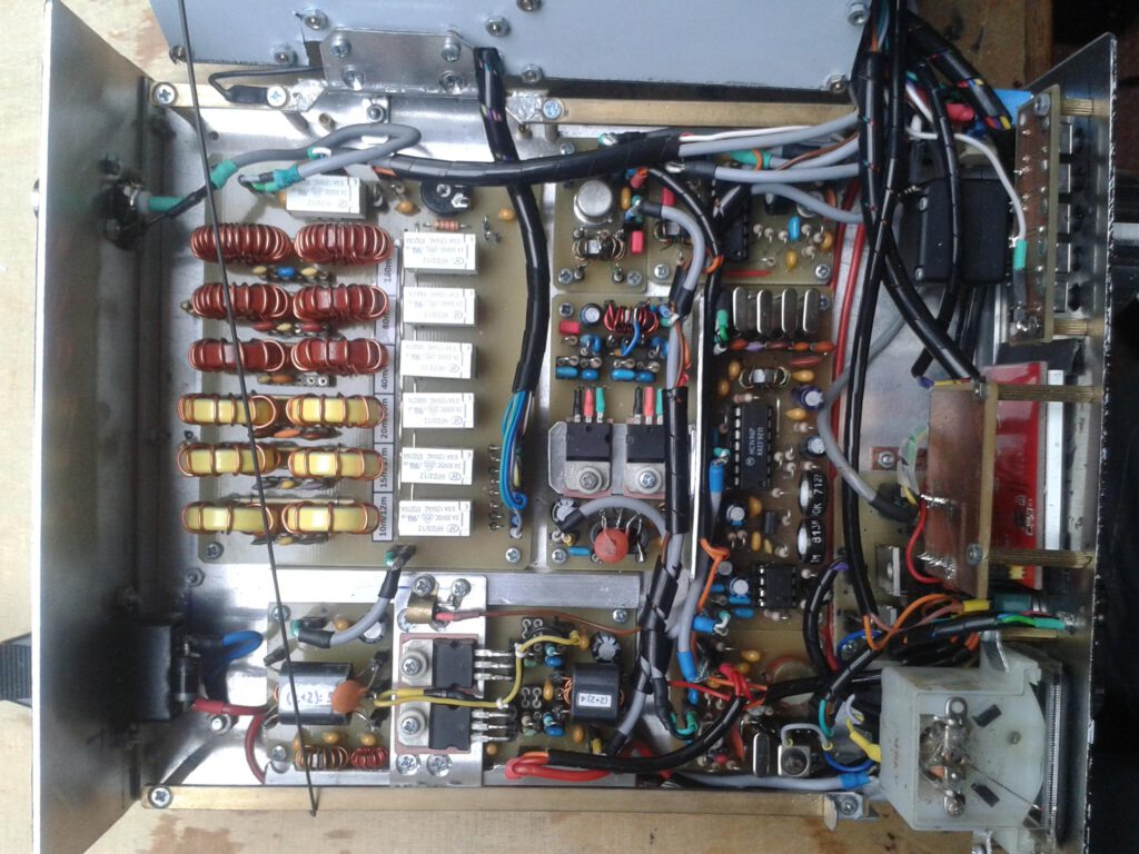
In the lower section we can see the local oscillator (just below the meter sited in the right front corner), the SSB generator above, the transmit mixer (again above), the various stages of the power transmitter (centered and on the bottom of the picture) and, last but not least, the low-pass output filter section with the transmit/receive antenna relay.
The DC power switching for T/R is hidden below the LCD board on the right side.
The single modules of the radio
As this has been a fairly complex project with uncertain outcomes I decided to minimize the risk of a total failure by separating the full circuit into single modules. We start this description with the receiver circuits:
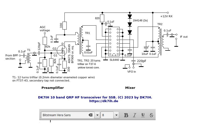
Module 1: Receiver front end
The receiver input takes the antenna input signals from the 10 band pass filter circuits described later in module 4. The first stage of the receiver strip is a broadband radiofrequency amplifier with a dual gate MOSFET as active component which ensures high stability even with strong signals, low noise and significant amplification in the range of 12 to 15dB. It is also part of the automatic gain control (AGC) chain.
The receive mixer applied here is an IC SL6440 which has been selected due to its outstanding IMD performance (about 30dB). It is a little bit more noise compared to the NE602 but capable of coping with high signal levels without producing intermodulation frequencies.
The PCB for this module:
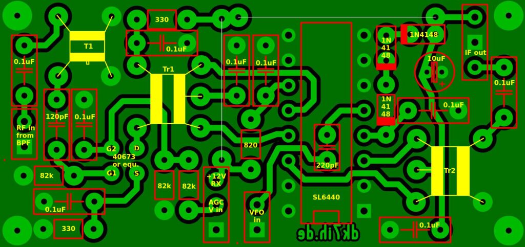
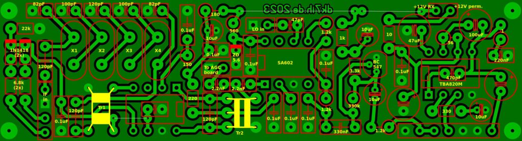
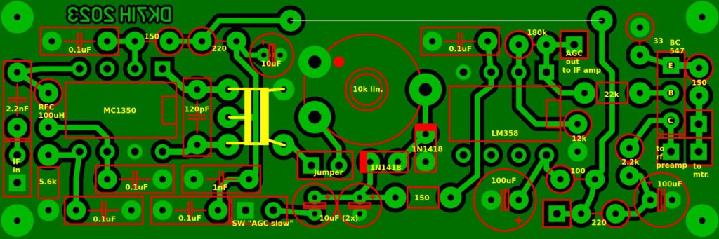
Module 2 – Receiver IF, demodulator and audio amplifier
This main receiver section module hosts a ladder filter consisting of 4 crystals (f=9MHz), the interfrequency main amplifier (IC=MC1350), the demodulator IC (SA602), an audio preamp (BC547) and the final audio stage, a TBA820M which has been preferred to the LM386 because of its improved output waveform and lower distortion.
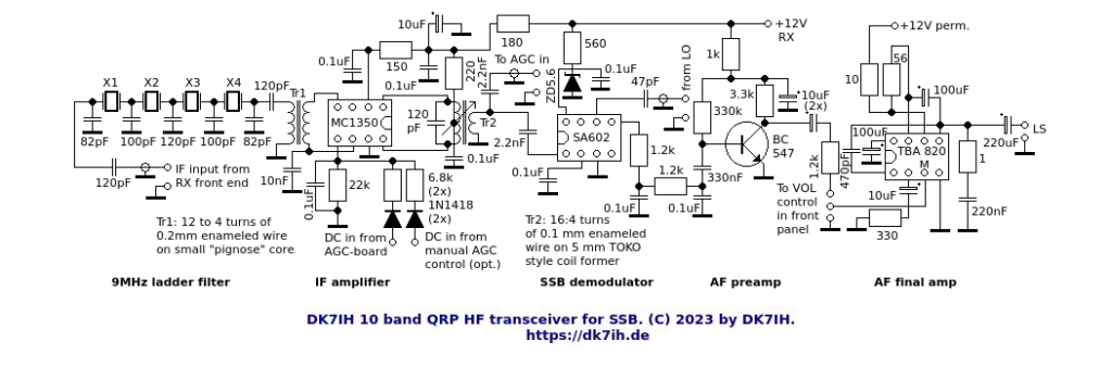
The PCB for this module:
Module 3: The automatic gain control unit for the receiver (AGC)
In contrast to my previous designs I tried a first-time use of an interfrequency derived AGC circuit. The amplifier receives the IF signal from the IF main amp and is also an MC1350 video amplifier IC by Motorola. This IC is not regulated and amplifies to the full possible gain of about 60dB. A rectifier unit follows a tuned circuit and an AGC hold circuit is integrated with a switchable second capacitor to prolong hold time of the AGC voltage. The DC voltage resulting from the radio signal then is amplified in a DC amplifier (OP LM358) whose output is fed into pin 5 of the main IF amplifier. Also there is a DC inverter stage for the contrary voltage characteristics of the dual-gate MOSFET sited in the entrance section of the receiver.
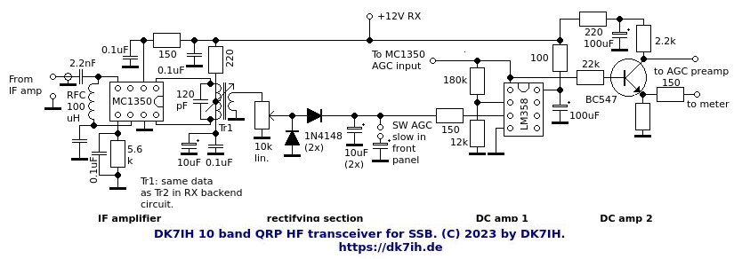
The respective PCB:
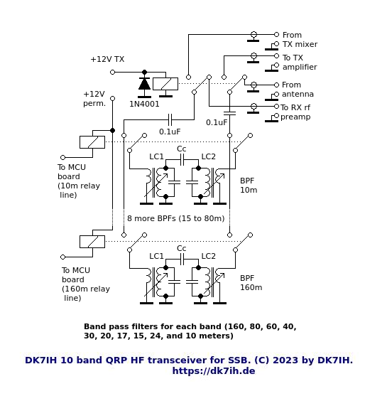
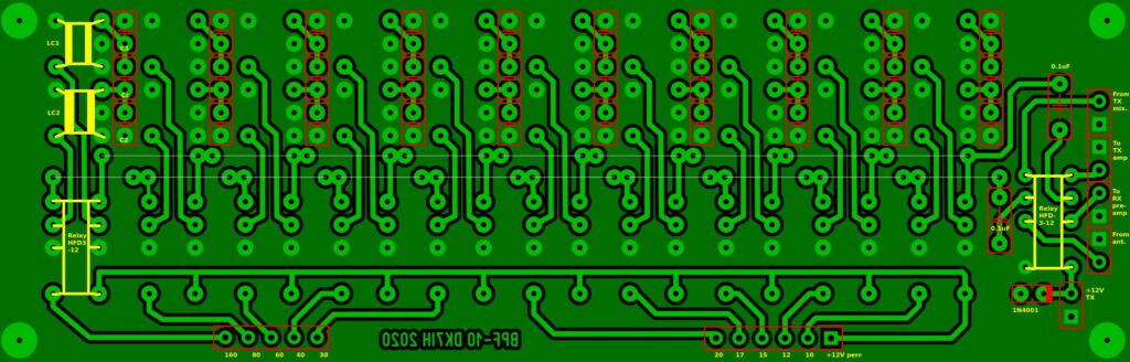
Module 4: Band filter unit used for receive and transmit
This section consists of 10 separate dual LC circuits that are switched by micro relays (HFD3-12). I prefer the the relays mainly because I have got a large number on stock because a bulk buy some years ago. These are driven by the well-known ULN2003 IC motor driver sited on the microcontroller (MCU) board.
There is also a relay on this board to switch the unit from receive to transmit mode and vice versa.
The PCB:
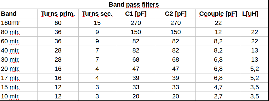
The data for the TOKO style filters and the parallel capacitors:
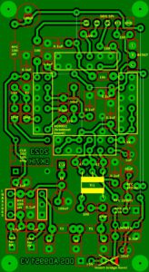
Module 5: The DDS VFO
The core part of the VFO is an AD9951 DDS chip by Analog Devices. It is clocked to 400 MHz which is the maximum clock rate for this device. The DDS output is succeeded by a monolithic 1.5GHz amplifier, an INA52063 by HP.
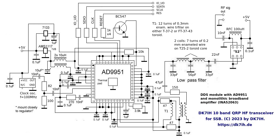
The output is symmetric to achieve a higher rf voltage and to ensure optimized performance of the DDS chip. A low pass filter (cut off frequency about 50MHz) terminates the DDS circuit, then the INA52063 follows to give a constant output voltage of about 1Vpp over the full frequency range from about 11 to 39 MHz.
PCB on the right: The AD9951 is mounted to 44 lead breakout baord.
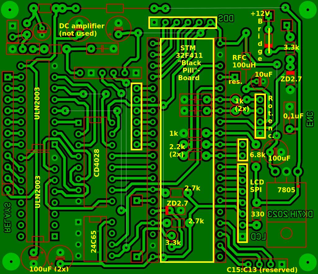
Module 6: The microcontroller (MCU)
The MCU used here is an STM32F411 on a breakout board, named “Black pill board”. It is clocked by software to 168MHz, the max. clock frequency for this controller. It provides 3 ports (PA, PB and PC) with 16 bits accessible in the most cases. The total number of available ports all in all is very much suffice for this project.
The band relay switching uses 4 MCU ports. A BCD decoder IC (CA4028) expands the 4 lines to a total of ten so that 10 band relays can be switched by using ULN20034 driver IC which holds internal clamp diodes. Some ports are accessible (e. g. the I²C ports on PCB6, PCB) for later use. Also some other ports are held unused for adding another LCD that is driven in parallel.
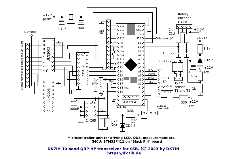
The PCB:
Module 7: The local (carrier) oscillator
This is a fairly simple circuit in Colpitts mode. It uses one 9MHz crystal. The respective sideband is tuned in by using either a series capacitor or a (tapped) series coil. A buffer is added after the oscillator stage.
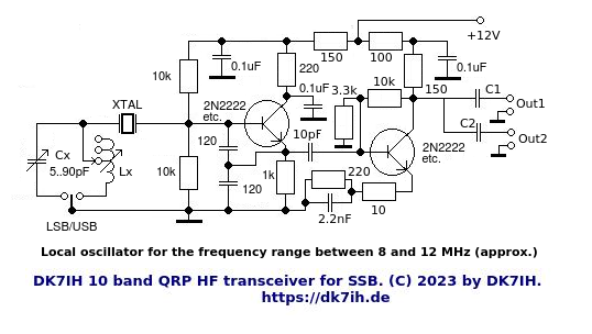
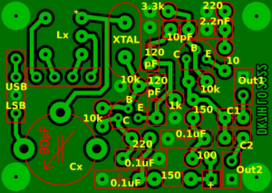
The PCB:
Module 8: SSB generator
An MC1496 has been used due to its excellent performance concerning carrier and sideband suppression:
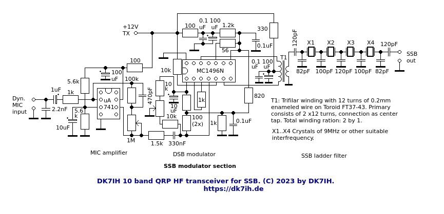
The microphone amp is designed for using a dynamic microphone and uses an operational amplifier type uA741. This amplified audio signal is fed into the MC1496. The DSB signal is coupled out symmetrically and then lead into a 4-pole ladder filter (f=9MHz). The resulting SSB signal has excellent performance with about 50dB carrier suppression and 60 dB unwanted sideband elimination.
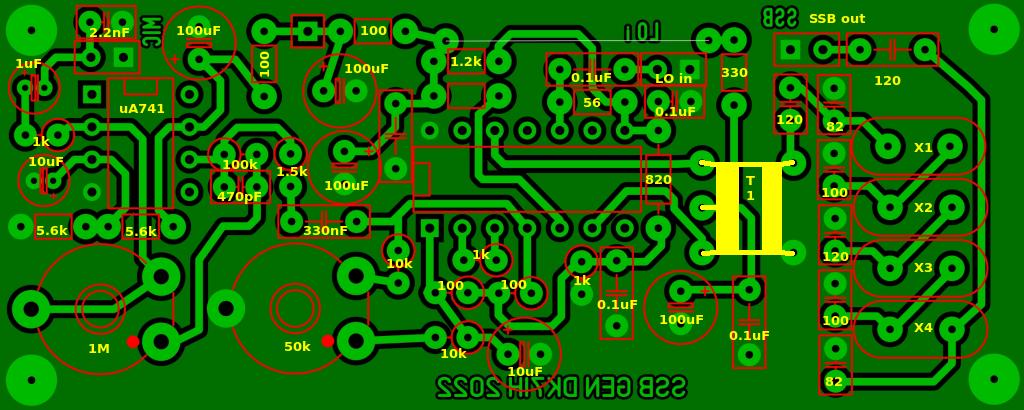
PCB:
Module 9: Transmit mixer
This mixer also is built using an MC1496N. The SSB input goes to a linear preamplifier (2N2222) and subsequently into the IC. Output again is symmetrically to a broadband transformer and then put into the band pass filter unit (module 4).
Rf output voltage is very high, about 3Vpp. are provided.
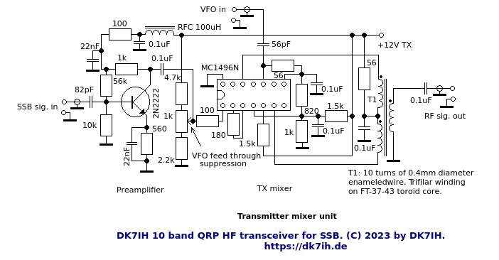
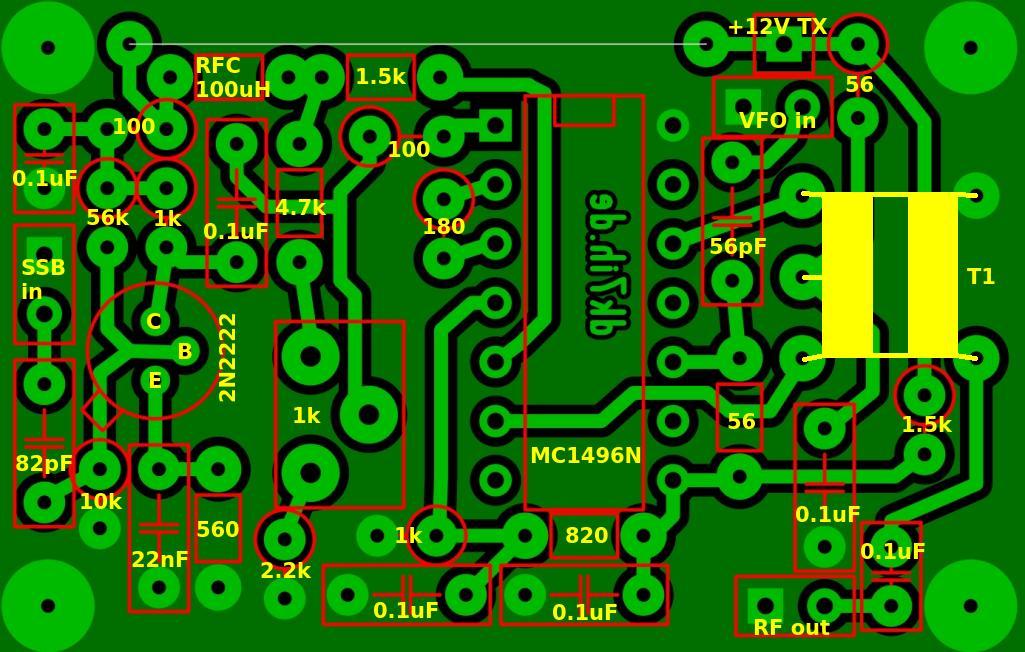
PCB:
Module 10: Transmitter amplifier stage #1 (Preamp)
Due to the high TX mixer output voltage there is no real preamp. Thus we declare this stage (which in other transmitters is the second stage, as “preamplifier”. It uses an 2N3866 bipolar rf transistor with emitter degeneration and negative feedback. It works using mode “A”.
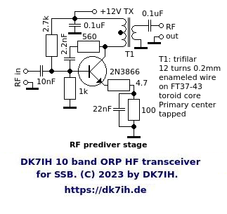
Output power is in the range of 400mW (50Ω)
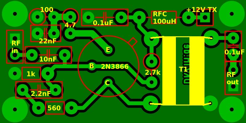
The PCB:
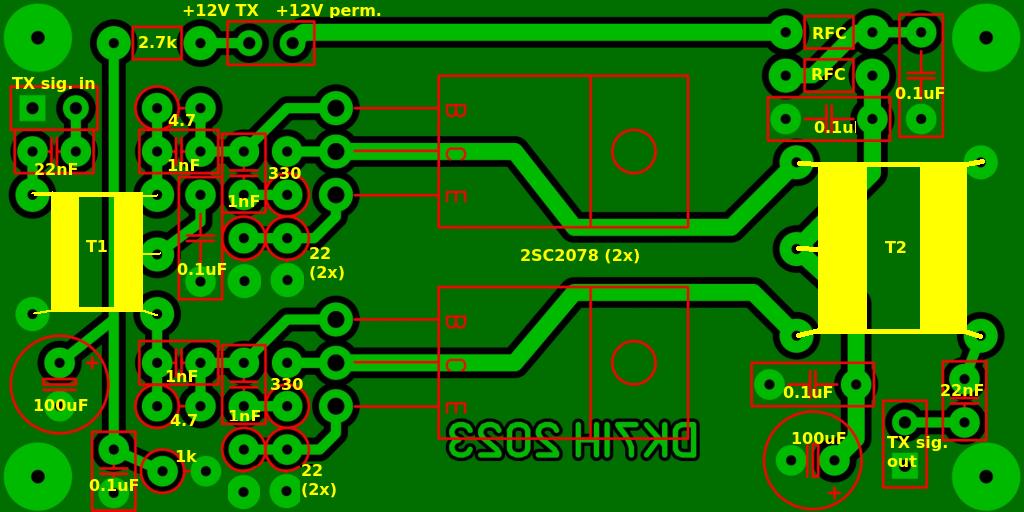
Module 11: Transmitter amplifier stage #2 (Driver)
The driver is in push-pull mode using bipolar rf power transistors (type 2SC2078) also using mode “A”. As with the stage before there is also emitter degeneration and negative feedback for linearity and to keep frequency gain relatively constant over the frequency range of the radio.
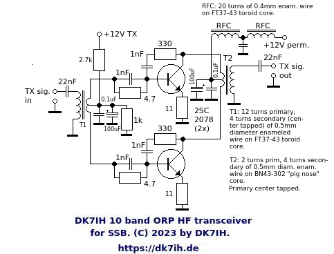
PCB:
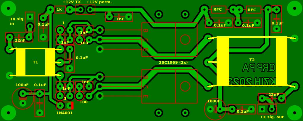
Module 12: Final rf amplifier (Stage #3)
This circuit is very similar to the previous stage. It is also a push-pull circuit, this time using 2SC1969 rf power transistors. The operation this time is in “AB” mode.
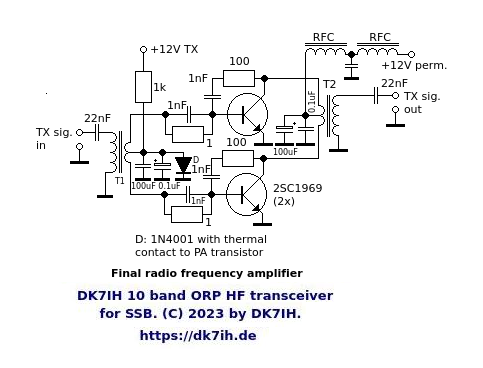
There only is negative feedback from collector to base, the emitters of the transistors are directly connected to GND.
PCB:
Module 13: The transmitter low pass filter (LPF)
For a 10-band transceiver it is recommended to use certain LPFs for at least two bands. This onset has been used in this module:
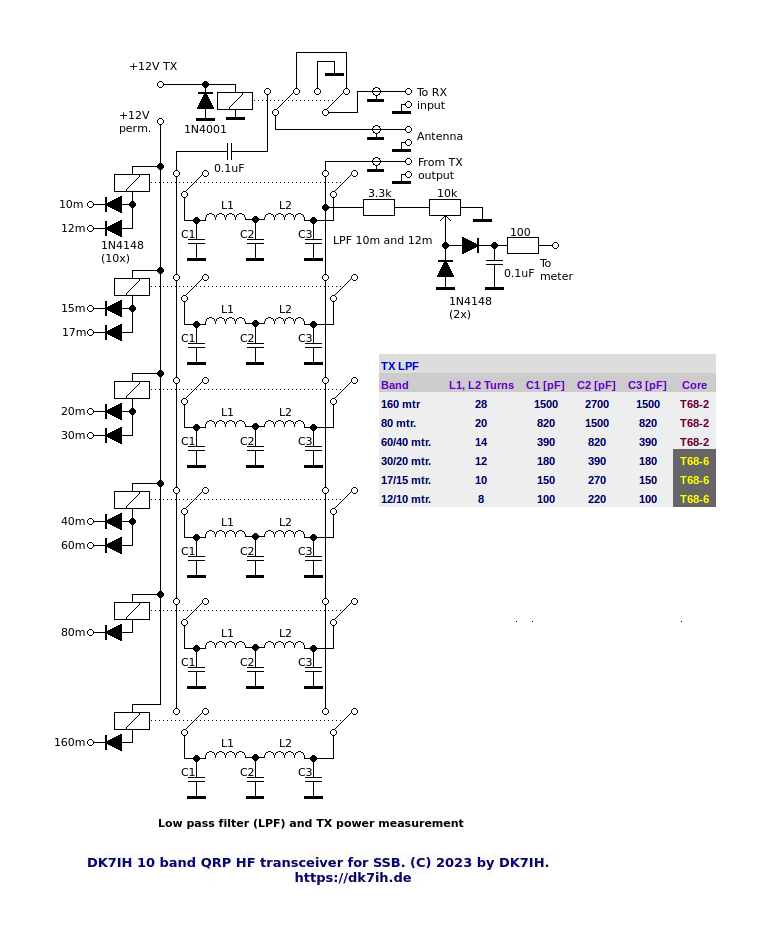
Also there is a measurement section on board to derive the transmitter’s power to the meter in the front panel. As well there is an antenna relay switching the antenna jack either to the receiver strip or the transmitter output. In case of transmit mode the antenna input of the receiver is grounded to avoid stray energy coupling into the band filter and thus generating unwanted oscillations.
PCB:
Module 15: T/R DC switch board
To avoid using more relays this board has been built with high-power MOSFETs of IRF 9340 type:
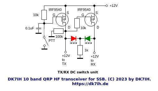
This module only switches the “low power” sections of the radio. The collectors of transmitter stage #2 and #3 are connected directly tho the input voltage that is equipped with a false polarity protection using a strong silicone diode.
Performance:
VFO: Due to the high clock frequency and the fact that the VFO frequency always is above the receiving frequency the number of spurious signals is very low.
Receiver: The rx of the radio has a very smooth sound. The AGC reacts ultra fast and there are no “pops” when strong signals come suddenly in.
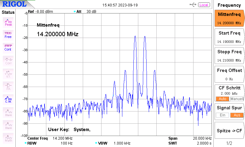
Transmitter: The TX power is fairly high, it exceeds the promised 10 watts by far:
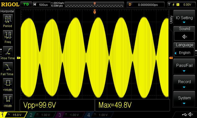
Here 25 watts PEP are reached. IMD3 of the same signal is in the range of -30dB:
Final thoughts:
The construction of this transceiver took about 1 year from the first thoughts on the VFO to the first QSO. The whole project turned out to be success and not, as I first was afraid of, a total failure. Much time has been, on the other hand, spent on optimizing the transmitter whereas the receiver worked from scratch.
Thanks for reading and vy 73 de Peter (DK7IH)