In this paper we will discuss a single sideband amateur radio transmitter/receiver for the 40 meter band that has been designed to ensure good performance characteristics with reasonable number of parts (no “overkill” in component use), particularly concerning the receiver. Circuit simplicity and over-average performance were to be combined.
The background: Some years ago I had built the ancestor of this transceiver and afterwards pageed an incomplete series of articles (starting here). The transmitter was considered to be quite OK (I could even work a station from South Korea when operating as GJ/DK7IH some years ago) but the receiver was weak.
The shortcomings originated from the rf preamplifier I used together with the 1st mixer, an NE602. The latter had severe problems to cope with the high signal levels on the 40 meter band from out-of-band broadcast stations transmitting on the 41m band (f>7200kHz) or from very strong amateur stations transmitting in-band. This is caused by the technical specs of this Gilbert cell mixer. NE602 has been designed for mobile phone applications and not for shortwave radios. Its IMD 3 is only -15dBm whereas it is able to detect weak signals (-119dBm with an S/N ratio of 12 dB) according to datasheet. Due to this NE602 was excluded from being used at least in the receiver.
Another point was that the rig was too small and too densely packed to be called “service friendly”. Thus I dismantled the radio some times afterwards and had in mind rebuilding it with another receiver and a little bit more space inside.
The Basics
The project has had to meet certain requirements that I would like to point out first:
Frequency generation: Dual-DDS-System: AD9835 as local oscillator and AD9834 as VFO. ATMega644A as MCU (Download source code here)
Receiver: Single conversion superhet, 9 MHz interfrequency with off-the-shelf filter (supplied by http://box73.de) shared by transmitter and receiver and relay switched, “NE 602-free zone” ;-), 4 dual gate MOSFETs in rf preamp, rx mixer, if amplifier and product detector, audio stages with BC547 as preamp and LM386 as main audio amplifier.
Edit: I found that there was strong signal of self-reception around 7.100kHz which was not a spurious signal from one of the DDS. It has been a mixing product of one or two oscillators together with a signal from the microcontroller. So I changed the interfrequency to 10.7MHz which cured the problem. I tried to calculate the issue but was not succcesful because I do not know all the frequencies in the microcontroller. I think it is most probable that it is a harmonic of the PWM signal I use for controlling the LED front lights.
Transmitter: 4 stages, 3 of them in push-pull mode, Siemens made mixer IC S042P (really old fashioned, but still available) as DSB generator and TX mixer, rf amplifiers (2N2219A) after filter and tx mixer.
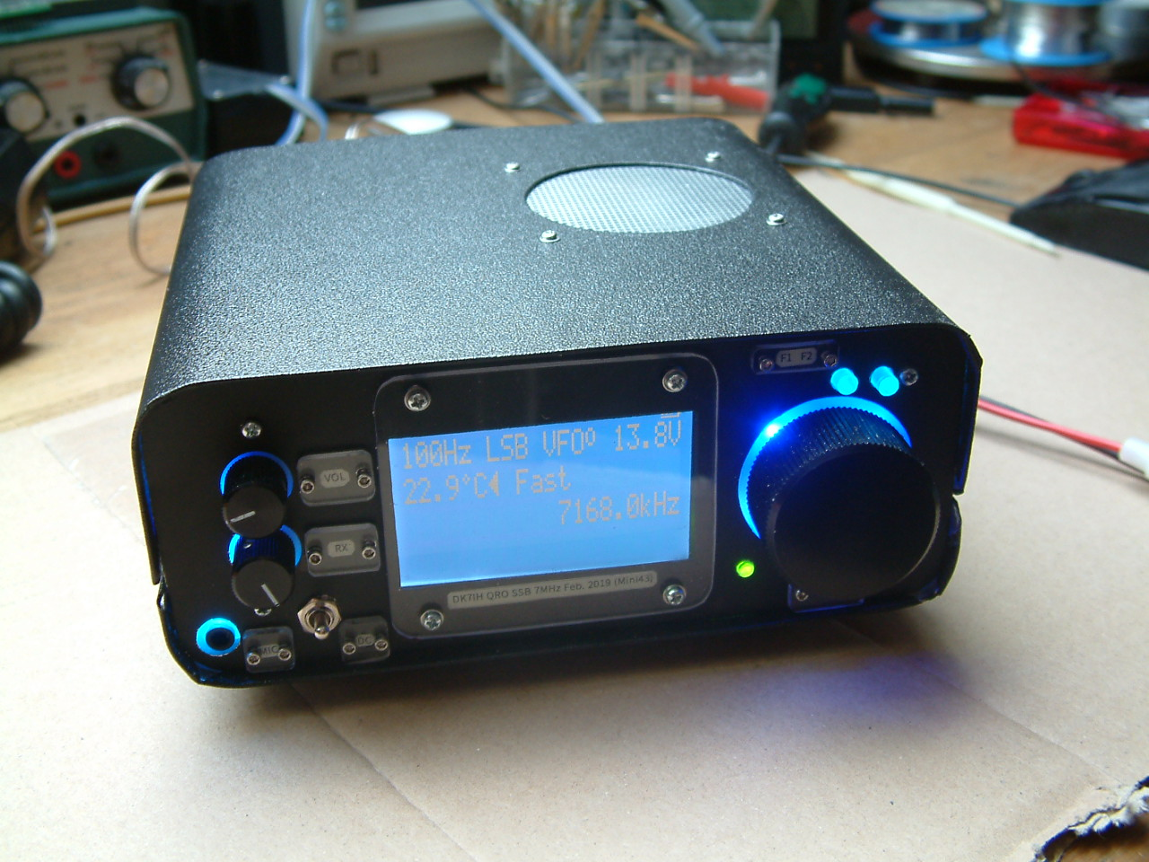
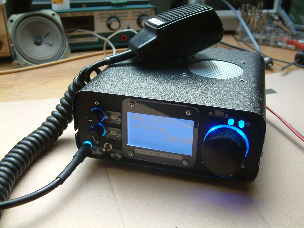
Design: Really “cool” with blue backlight. Sandwich built, not the size of a “micro transceiver”, but handy for travelling.
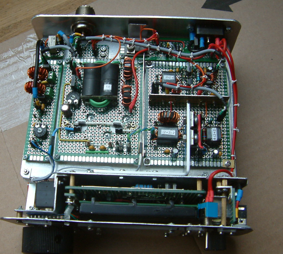
The Block Diagram
The diagram can be derived from the old project, it is nearly the same:
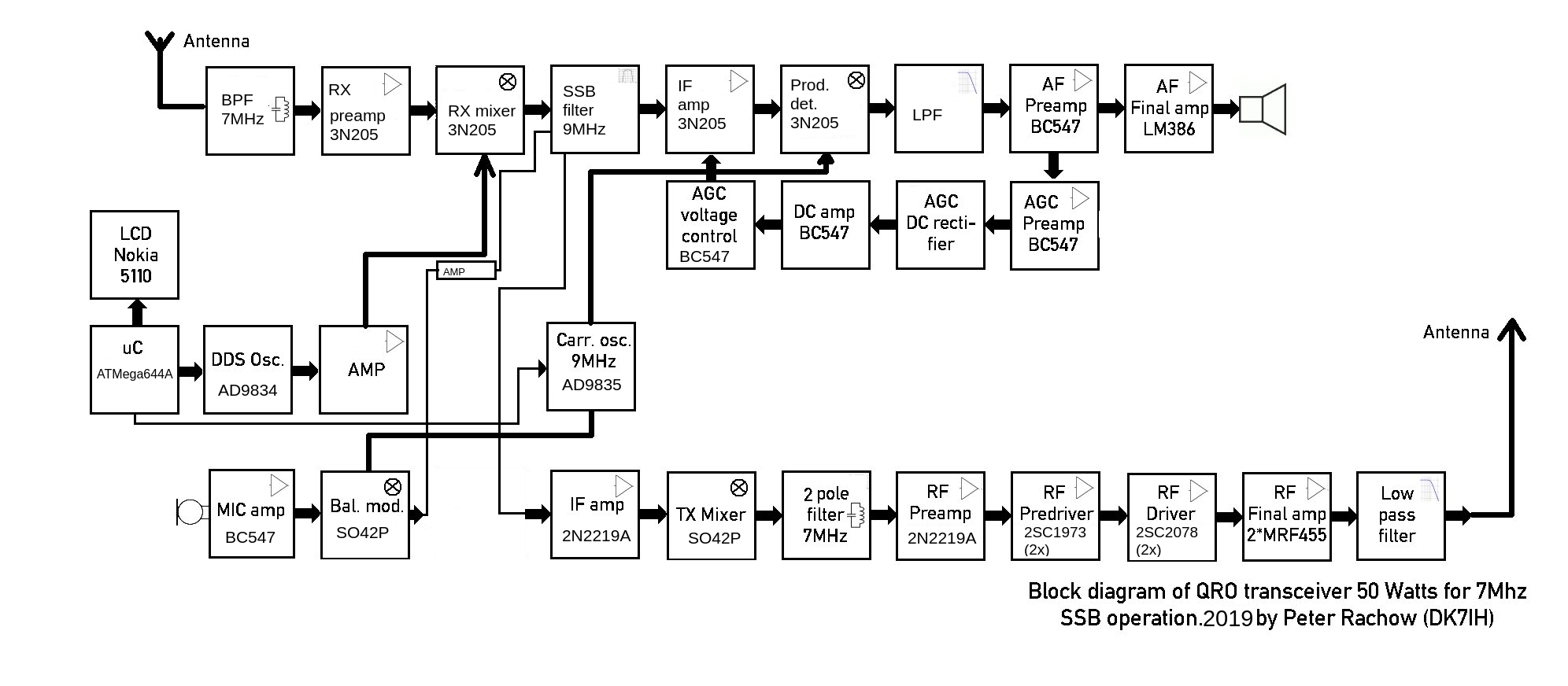
The basic outline of the radio is standard and should not be further discussed.
Dual DDS (VFO and Local Oscillator (LO))
This time I wanted to use 2 digital oscillators. The reason was just to have fun. 😉 Here is the schematic:
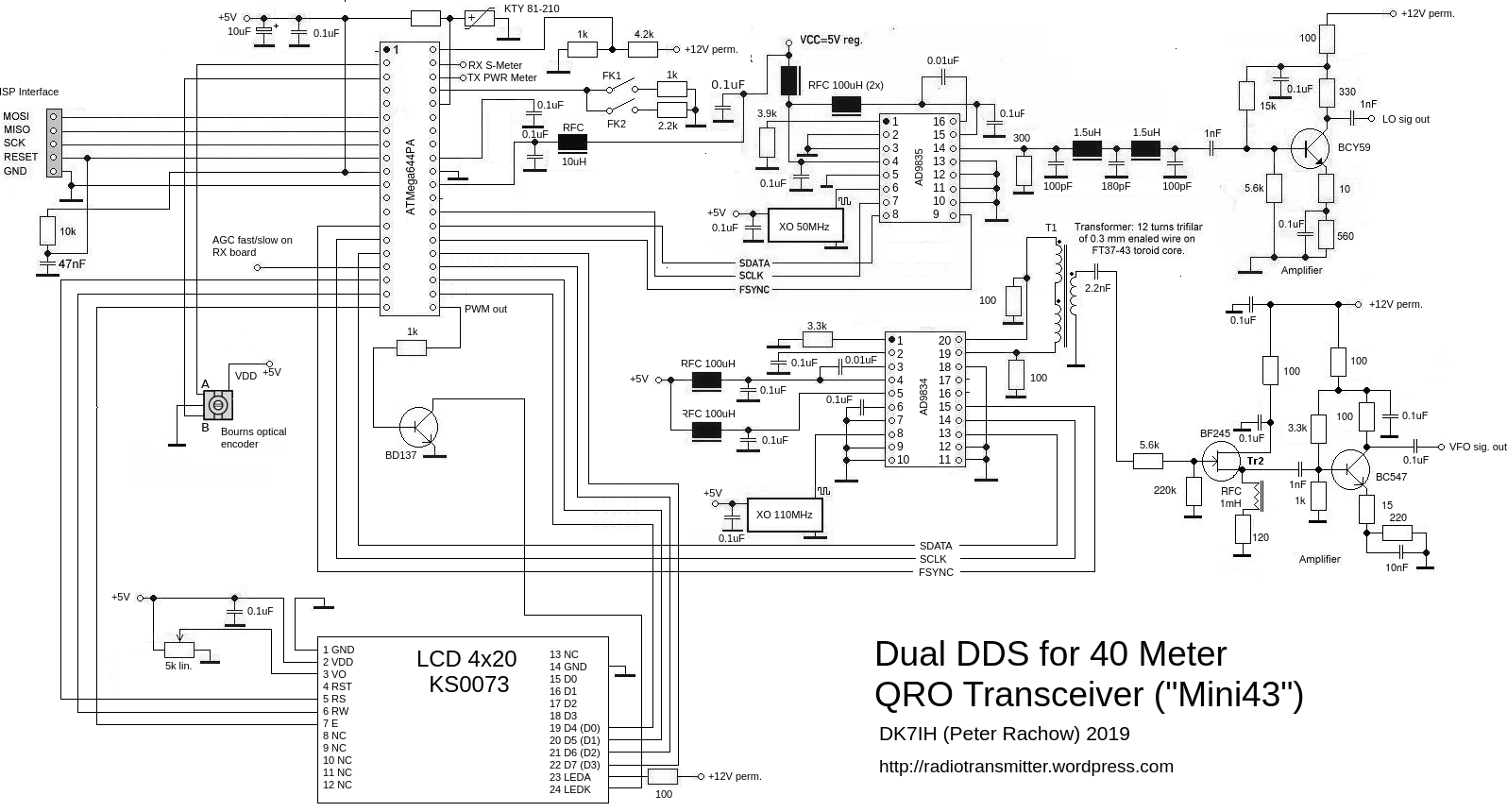
Microcontroller (MCU)
The source code has got about 2200 lines. With the GNU C compiler this leads to a HEX-file of about 43kB. Because of this the controller had to have a little bit of more memory. A “644” is a good choice here. It is clocked internally to 8 MHz clock rate. Radio and user data (user operated keys, S-Meter, TX PWR meter, temperature sensors attached to final transistors) is lead to the analog-digital-converter (ADC) of the MCU. Rotary encoder (optical) is fed into digital inputs. Integration of an RTC is projected but not done yet.
DDS1 (VFO)
Here an AD9834 is used. It is overclocked with 110MHz clock rate. For my receiver with a DDS chip purchased from Mouser this works without any abnormality. With a a chip from the “free market” (ebay) I found that there were strange clicks in the signal. So, I do not really recommend overclocking under any circumstance and/or not to such a high degree.
This DDS is is not terminated with a low pass filter. Due to the high clock rate there is no clock oscillator feedthrough which is supported by the design of the following amplifier having an audio frequency transistor in the last stage (BC547 and later BCY59) that limits high frequency components due to its early gain decay in the frequency spectrum. The two stage amplifier has been designed for excellent linearity to prevent impurities in output spectrum.
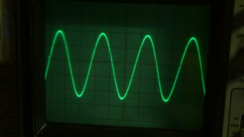
The first peak showing the 16MHz signal and the next peak is the first harmonic about 30dB below. Other peaks are from local sources (PC, Printer).
The sine wave also looks quite OK:
DDS2 (LO)
This one contains an AD9835 synthesizer clocked to 50 MHz. An LPF here is mandatory. A simple but linear amplifier brings the signal up to 3Vpp which is OK for driving the dual gate MOSFET in the receiver. For the transmitter mixers this amount of voltage is too high, small capacitors reduce the voltage to an acceptable value.
LCD
From another project that I once had built and that is not more in use, a dive computer, I had a 4 lines/20 characters text display that is fairly large. This was to be designated as the LCD for this transceiver.
The Receiver
Building a receiver for the 7MHz amateur band is challenging. On one hand the circuit should be very sensitive for weak signal reception, particularly during day when the band conditions are low due to solar radiation and density of the D-layer. This means the receiver should have a higher gain whereas noise figure does not play a predominant role due to band characteristics with high atmospheric noise on 7MHz.
Next request is high dynamic range to eliminate the spurious signals that occur when front end stages are loaded with high input signal levels.
And last but not least AGC control range should be as wide as possible to cope with weak and very strong signals without the request to intervene by adapting manual gain control. For this a preamp also benefits.
Active mixers like the NE602 show low performance under these conditions. Some high-current mixers like the SL6440 exist, but there are alternatives. On one hand the classical diode ring mixer might come into perspective, otherwise Dual-Gate MOSFETs are well known as having a fairly good ability to cope with high signal levels and so don’t tend to deteriorating the receiver’s performance severely. Besides they offer some gain and low noise figure (which has not been the main objective in this case) and the circuit is very compact and therefore it was the best choice for a receiver that had been intended to be constructed onto a board of 6 x 8 centimeters.
After these thoughts the following circuit turned out to be the right onset for a receiver inside the projected rig.
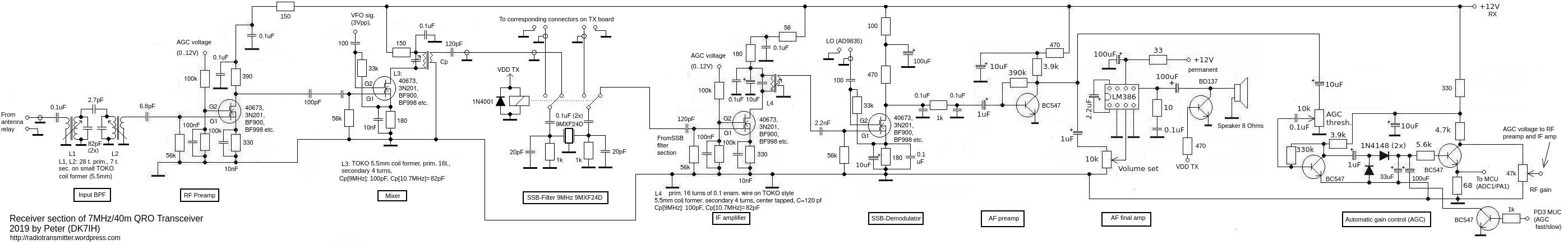
Circuit explanation (Receiver)
Front end
On the left we start with a 2 pole LC band pass filter for 7 MHz. The coils are wound on TOKO style coil formers (5.5mm size), winding data and parallel capacitors are given in the drawing. The coupling capacitor (2.7pF) between the two LC circuits is very small for such a low frequency. This makes the filter response curve sharper but leads to a slight weakening of the signal coming through the filter. But as the whole receiver has plenty of gain and a very good noise figure, this is the reason why some weakening of the input signal is acceptable.
Preamplifier
Next is the preamplifier for the received band. It is connected to the AGC chain. You can expect some 25 to 30dB gain swing by driving up gate 2 of the dual gate MOSFET from 0 V to 6V. A 1:1 voltage divider decrease the 0..12V AGC voltage to 0..6 V where th3N205 MOSFET is close to amplify with maximum gain. Exceeding 6 to 7 volts does not result in significant more gain swing, so I usually drive the MOSFET from 0 to 6.5 volts UG2 (with 13 Volts of supplied voltage.
The coupling when going from the preamplifier to the receiver mixer is in broadband style. The 3N205 has a very high gain and tends to self-oscillate. A second LC circuit makes the device more prone to going self-resonant and hence produce unwanted signals.
RX mixer
This mixer is very simple and needs only a few components. Both signals are fed into the gates of the dual gate MOSFET. Rf goes to gate 1 whereas gate 2 (the AGC input) is fed with the oscillator signal). Gate voltage depends on the voltage drop at the source resistor and therefore is stabilized. The oscillator signal should be in the range of 2 to 3 volts rf (pp) for a dual gate MOSFET. Lower values will deteriorate the performance of the mixer, e. g. its dynamic range. This signal switches the semiconductor and a superposition of the two signals occurs thus leading to the production of sum and difference of the original frequencies. These signals are fed into…
The SSB filter
which is a off-the-shelf one (Supplier box.73.de). The reason why I don’t ladder filters anymore is that I found it extremely difficult (not to say impossible) to get a symmetric filter response curve thus making the lower and upper sideband of the receiver sounding different even when the carrier frequency has been adjusted very thoroughly.
The filter is used for the SSB transmitter as well. To ensure maximum signal separation between the two branches (tx and rx) and between filter input and output I again us a high quality rf relay made by Teledyne. When choosing a relay intercontact capacitance is crucial. It should (if possible) be < 1 pF.
Don’t forget a clamp diode to VDD over the relay coil to eliminate high voltage voltage peaks generated by self inductance when the coil is switched off. Voltages up to 100 Volts can occur. This might damage the transmit-receive section of this transceiver that is equipped with semiconductors only and does not use a relay.
IF amplifier
This circuit is the same like that of the rf preamp. It also is part of the AGC chain, thus delivering another 25 to 30 dBs of gain swing so that overall gain swing is around 50 to 60dB. In practical research over a long period of observation I found that with an antenna delivering high signal voltage (Delta loop) it was not possible to overdrive the receiver to a level where signal distortion was audible.
A tuned circuit is also placed here to increase gain. Tuned amplifiers usually have higher gain than broadband ones. It is highly recommended to ground the metal cans of the coil to prevent any self-oscillation. But as I found out, this amplifier is not very prone to go to self-oscillation state.
Product detector
Here again a dual gate MOSFET is used. The circuit is nearly the same like the RX mixer except from the output section. We can see a low pass filter here, consisting of 2 Cs (0.1uF) and a resistor (1k). You can use a radio frequency choke instead, 1mH is recommended.
Audio amplifier
This section consists of two parts, a preamp (with bipolar BC547) and a final amplifier (LM386 IC). It is well-known that this IC tends to oscillate. One measure to prevent this is to keep leads short, switch a low-pass filter (capacitor 100uF and R=33Ω) into the VDD line and to reduce the gain capacitor between pins 1 and 8 to a degree where self-oscillations terminate.
A switching transistor cuts off the audio line by short circuiting it when on transmit. This eliminates any noise when switching. The rx/tx switch now is 100% “click free”. A very pleasant way of operation. 😉
AGC
This is another re-use of a circuit I have frequently used before. It is desired to reduce its output voltage down to 0 volts when a more or less strong af signals appear at the input. The agc voltage is derived from the audio signal of the receiver. Some say that this is not the best choice because you need more time (an af cycle last much longer as an rf cycle) for the waveform to generate the regulating DC voltage.
Nonetheless I have never observed popping or unpleasant noise from incoming very strong signals. The agc response rate is so fast that you won’t notice that it just has regulated even when a strong signal comes in. Only with very, very strong signals a slight “plopp” sound is observable but it is not unpleasant.
A second capacitor can be switched in parallel to the 33uF one. This can either be done by a transistor switch (like shown in the schematic) that in this case is controlled by an output PIN of the MCU. An alternative that I found later is to use the MCU pin directly to switch the cap. When not using the additional cap you must switch the pin as an input so that there is no positive voltage from the pin to the circuit. When you intend to ground the transistor (agc in “slow” position) then the pin mus be set as output by defining the DDR-register respectively AND the pin must be set to 0. So you can get rid of the switching transistor.
Another possibility would be to derive the agc from the interfrequency signal. The problem that occurs in this case is that you have to decouple the local oscillator (bfo) very carefully from the place where agc circuit is placed. Otherwise you are at risk to detect the bfo signal by the agc which leads to reduced response range in the agc. In addition this receiver uses a higher rf voltage level for the mixers (2 to 3 Vpp each). By this the amount of stray energy is higher inside the circuit and thus this rf energy might be detected very early by the agc.
In the emitter line there is a resistor (68Ω) which produces a voltage drop when the transistor is driven. This is fed into the ADC of the microcontroller driving the S-meter display part.
The Transmitter
First the circuit:
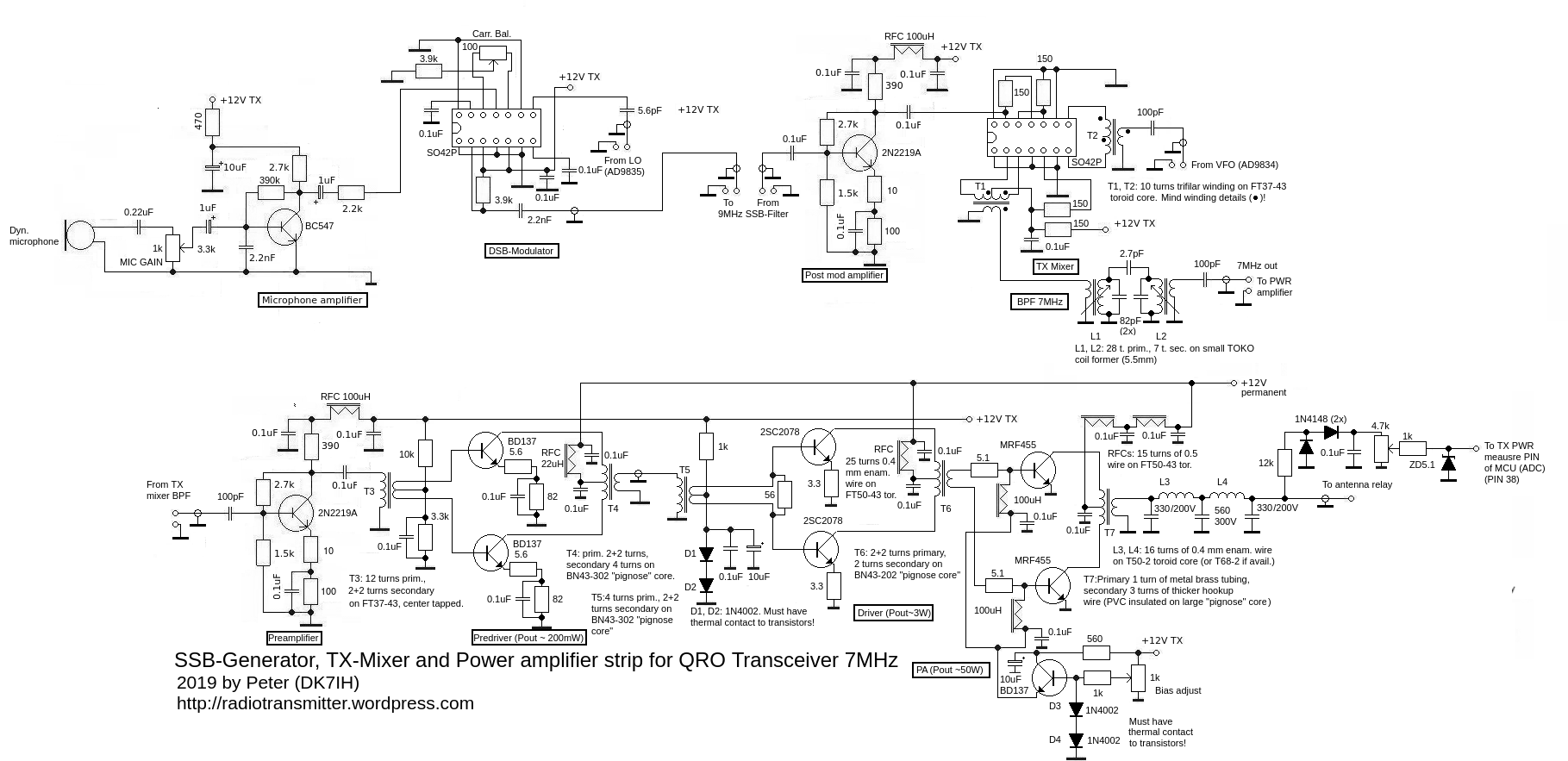
Microphone amplifier
This amplifier is a simple common-emitter circuit with the directly grounded emitter of the BC547 transistor. This circuit is linear only for low input voltages but suitable for the connected dynamic microphone since this does not produce more than some millivolts of audio energy. Bias comes from the 390kΩ resistor. At the input you find a 2.2nF capacitor from base to GND which helps to prevent coupling in rf energy from the transmitter to the audio stage and thus leading to an impure signal.
The DSB generator + amplifier
The amplified microphone signal is used to produce a double-sideband signal. The ic I use here is an antique but still available part by German manufacturer Siemens, the S042P. It includes a so-called “Gilbert-cell” mixer and an oscillator but the latter is not used here (Datasheet Application note (in German)).
The S042P mixer needs some more components compared to the well-known NE602 integrated circuit but fewer ones than the MC1496. It is designed for 12V usage, thus no voltage regulation is required.The ic can be applied in balanced mode or non-symmetrical. To save components I use the unbalanced circuit alternative. A slight loss in output power is acceptable in this case, there are amplifiers page each mixer in this transmitter.
Ic gain is about 16.5 dB, DC current is about 3 mA.
A crucial point is the signal level of the local oscillator. S042P needs only some hundred millivolts of oscillator voltage. To prevent overdriving I experimented with different values of the coupling capacitor. 5.6pF seemed best because the LO produces some volts peak-to-peak.
Following there is an amplifier that is a standard circuit and has been tuned for maximum linearity in order to reduce distortion to a minimum (which is also true for the following stages). You can see the well understood 2 master ways of achieving max. linearity in an amplifier stage:
- Negative feedback between collector and base (i)
- Emmitter degeneration (II)
Explanation:
i) The first measure goes along with the 2.7kΩ resistor between collector and base of the transistor. This resistor provides positive dc bias voltage to the base and leads 90° out-of-phase ac voltage to the transistor’s input. This reduces gain and therefore distortion. But due to the fact that the whole transmitter strip has plenty of gain, this loss in gain is not a serious problem.
ii) The 10Ω resistor in the emmitter line is not bypassed by a capacitor. This stabilizes the circuit. When the current through transistor increases the emmitter voltage will rise (according to Ohm’s law) and the voltage between collector and emmitter drops. This reduces voltage difference between base and emmitter and hence also reduces gain.
The coupling to the next stage is done by a capacitor of 0.1uF. This causes some impedance mismatch. But that is as well not a big problem because the gain reduction here helps to prevent the whole transmitter from unwanted oscillations by diminishing overall gain.
TX mixer
Here the second S042P is used. The 9 MHz SSB signal is coupled to pin 13 of the ic, a DC connection is established to pin 11. These two pins represent the base connectors for the two current control transistors and should be bridged by a DC resistor in this circuit.
The 150Ω resistor from pin 10 and pin 12 to GND defines the gain of the mixer. Here you can use down to 150Ω but should have a resistor towards VDD to limit current and avoid excessive heating of the device. In this case another 150Ω is used.
VFO signal is coupled symmetrically to pins 7 and 8 via a small trifilar toroid. See schematic for details and please note that center tap is not used here. This is in contrast to the output transformer where the tap is used to feed supply voltage into the mixer.
Another 7 MHz band pass filter terminates the mixer, data for coils and capacitors is in the schematic.
Power amplifier
This amplifier has got 4 stages and except from the first one all are in push-pull mode. The power distribution for these 4 stages is as follows:
| Stage | Power |
| Preamp | 5mW |
| Predriver | 200mW |
| Driver | 2.5 W |
| Final amp | 50W |
Preamplifier
The first of the 4 power stages is the same as the page dsb generator amplifier so there is not more to add concerning this stage. Rf energy is taken out via a transformer with a primary and a tapped secondary winding. This is to provide the balanced structure necessary for the following push-pull stage.
Prediver
This is the first push-pull stage. Its bias is derived from a voltage divider connected to the tap of the input transformer.
Please note: In contrary to the schematic I have installed 2 devices of the 2SC1973 type because the signal turned out to be much purer with these ones on the spectrum analyzer.
A tapped output transformer feeds the amplified rf energy to next board. Output impedance is 50Ω. The coupling to next stage then is done via a shielded cable of (nearly) the same impedance.
Driver stage
This one has an input transformer also center tapped. The tap goes to a bias network consisting of a current limiting resistor (1kΩ), two diodes forming the lower part of a voltage divider and some capacitors as part of a low pass filter to avoid coupling in of radio frequency (rf) energy. The two diodes must be thermally connected to the cases of the transistors. In case these heat up, the diode increases its conductivity thus reducing its resistance. The bias voltage drops and heating is stopped. So, thermal runaway is prevented.
For these two stages (predriver and driver) DC is fed through low pass filter (RFC and 2 caps 0.1uF) to prevent coupling of rf energy via the VDD line.
Final stage
This stage receives input from a balanced structure without a center fed transformer. Instead bias current is linked in via a network of radio frequency chokes and two resistors of 5.1Ω each.
Bias is provided by a current regulating transistor and should be set to about 100mA.
The MRF455 transistors are mounted directly to the aluminium structure of the sheet metal carrying the whole transceiver boards. When mounting them to the Veroboard I did not solder them directly. I used 1.6mm screws and washers to press the brass connectors to the copper strips of the amplifier board:
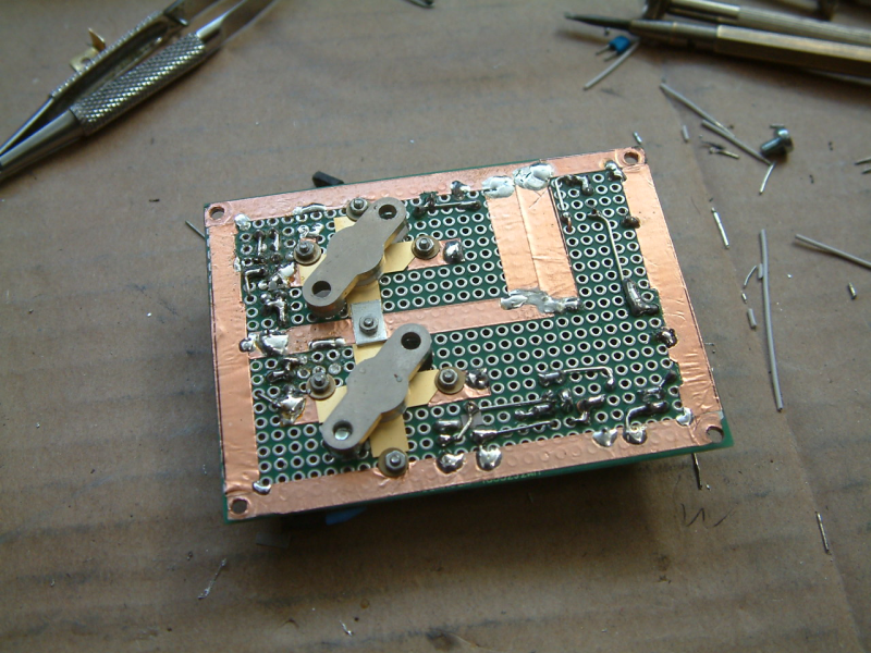
With this I could have been able to remove the precious transistors without having to unsolder them when the device might have turned out to be a failure. But it was not, thank God!
The output transformer is the one I have used in my old 14MHz PA and the ancestor of this radio. It is from an old ATLAS 215 transceiver and I hope that this will be the final place for the transformer.
Two temperature sensors (KTY-81-210) have been installed to measure the temperature of each transistor. They are connected to the microcontroller via voltage dividers (see schematic, please!)
Low Pass Filter and Power Measurement Unit
For the low pass filter I use 2 toroids T50-2. These might appear small but from one source (that I have forgotten) I remember to have found that for 50 watts of power this core is still suffice. Metal powder cores can stand much more power compared with same sized ferrite toroids.
The power measurement unit consists of a network that starts with a resistor of 12kΩ to ensure a significant voltage drop in signal level, then two rectifier diodes (1N1418 or equivalent) follow, some low pass filtering eliminating the last rf energy and the resulting direct current voltage is fed to a variable resistor to set an adequate voltage level for the ADC in the microcontroller.
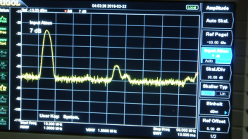
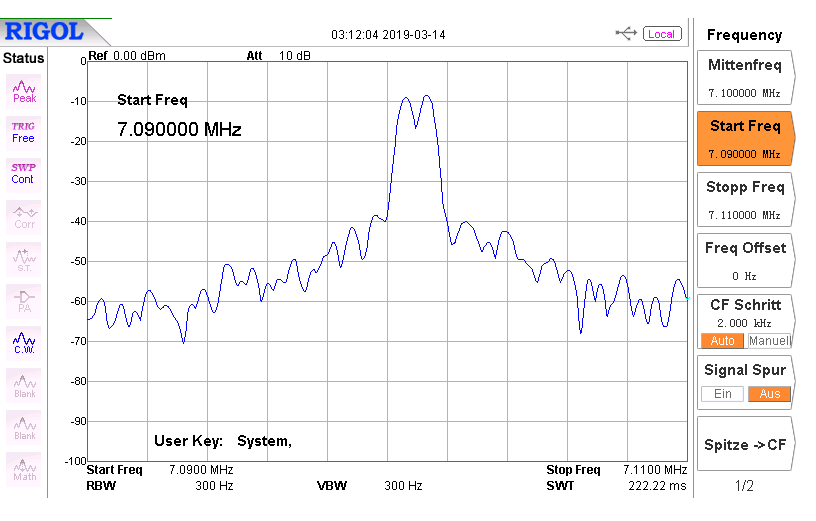
The rf output made out of a two-tone audio signal measured at the antenna connector:
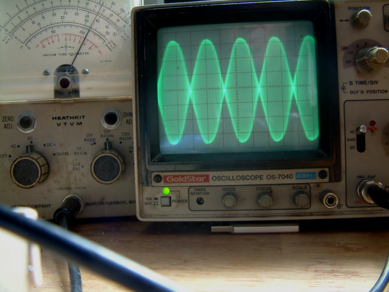
The spectroscopical analysis shows the signal on the f -> V figure:
RX/TX-switching
A very simple circuit. Two PNP power transistors are used but they don’t have that much to do. They are only designed for switching the low-power parts of the radio. The high current to the drivers and final amplifiers is permanently present in the collector lines but the bias lines are tx/rx-switched and go to 0V during receive periods. This reduces requirements for the power rating of the switch board.
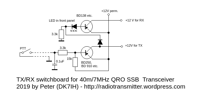
When pushing the PTT the base of the lower transistor is pulled to GND. So it becomes conductive and TX DC is applied. Via the diode the upper transistor loses its negative voltage and becomes non-conductive.
Construction
The Backlight
One interesting thing was the blue backlight to illuminate the front panel controls. It is made using SMD LEDs that are soldered to small pieces of Veroboard and fixed with 2-component glue to transparent light-scattering plastic bought from a local supplier for architects and designers. This material is used for making models of houses and stuff like that. As light distributor this material is excellent. The LEDs are powered by a linear transistor connected to the pulse width modulation (PWM) output of the microcontroller so that light intensity is adjustable.
Hint: When programming the PWM functions it might occur that PWM frequency is audible in the receiver. If something like that occurs another frequency can be selected without changing the performance as soon as it is high enough that human eyes aren’t able to recognize a flickering.
The covers used for the labels and the LCD shield are made from 2mm acrylic and fixed with screws of 1.6 respective 2mm diameter.
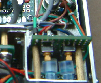
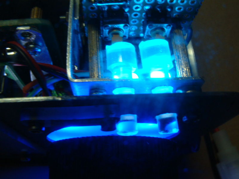
The two push-buttons right in top position consist of two bars of acrylic (4.2mm diameter) and are having mechanical contact to small spring-loaded switches behind the front panel:
Directly under these acrylic bars there are two LEDs shining into these rods and because of total reflection inside the tubing the optic conductor is sending the light to the front side when the LEDs are powered on. That is how it looks at night:
General setup
This is a sandwich construction again. On the first side there is the DDS board (left), the receiver (center) TX mixer and preamplifier (right) and the SSB generator (back). Also there is a 5 lead connector holding the 5 ISP lines (MOSI, MISO, CLK, RESET and GND). This makes firmware updates easy because you don’t have to open the case when you want to update software.
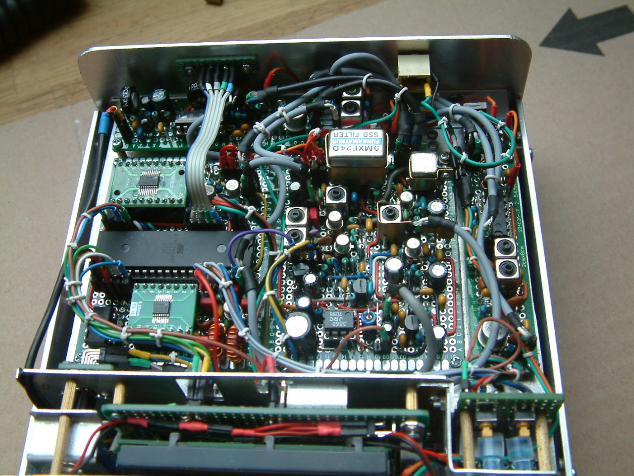
The other side holds the TX low pass filter plus power measurement unit (left), the power amplifier (center) and the predriver and driver (right). In the back you can see the rx/tx switch board:
“On the air”
Again big fun this transceiver! During the ARRL DX contest last weekend I could work some statesiders. With Delta Loop and 50 watts, fairly OK. Working Europe all day is no problem with 50 watts.
During the first QSOs I had reports that the audio sounded clear but somehow “narrow”. I had used an electret mike that time and could not use a dynamic one because the preamplifier following the microphone did not have enough gain. Then, to solve this problem, I decided to do a full reconstruction of the SSB generator board. The one then had used had an AN612 mixer integrated circuit (from an old CB radio). This one was dismantled and replaced by the S042P board. The change took me 3 hours to develop and solder but it paid. I use a Motorola dynamic microphone now that has a very rich and clean sound. I monitored it on a web based SDR receiver, made a recording and found it to be OK.
OK, dear fellow hams, that’s the story so far, some supplements will sure be made, so stay tuned!
Thanks for reading and vy 73 de
Peter (DK7IH)
Great work, Peter!! Go on working!!!73!
Nice project.
But very nice if share for firmware and schematic.
Hehe
Love reading of your builds Peter, much to learn from your accounts, a celebration of the spirit of homebrew, keep designing and building, keep the craft alive! Very best 73 from down under, Paul VK3HN.
Thanks a lot for your post Paul and Ciro! Best 73!
A few specific comments Peter, now that I’ve had time to read thru the post and study the circuits. Firstly, I am bemused as to people consistently reporting SA612 mixers suffering strong signal overload. I am currently using two receivers with SA612 mixers, one with RF amp and one without (one is a build of your Micro40 txcvr for 4 bands, blog post soon).
Neither exhibit any rx overload as far as I can tell with my ears. I also have three other homebrew rx’s using diode mixers. I cannot tell any difference between them, even with an adjacent s9+30db station. If the artefact of poor IP3 is a rise in general background noise, then this is not noticeable to my ear. One possible explanation is that I live in a part of the world with low ham density and under a 400w PEP power limit. Another is that my 80 and 40m dipoles are not overloading my receivers like a higher gain antenna may. Also, the nearest shortwave BC sources around 40m are in Asia and not excessively loud. Perhaps all these factors combine to make VK3 a ‘NE602 friendly’ region. I will continue to use SA612s as they are such useful mixers.
To your build. You got a lot of gain out of your 3N205 stage. I have always had dual gate MOSFETs oscillate at the slightest touch, so in my latest build, used them untuned and with conservative gain settings, around 12dB. I found that screening and decoupling help only so much, and the best way to tame them is to reduce gain. MOSFET RF amps are prone to instability at specific frequencies, less of a problem in the IF or a monobander.
I agree that homebrew crystal filters can take a lot of time and hit and miss experimentation to get to the desired bandwidth and to be symmetrical. My last effort (on 12MHz, in my DK7IH Micro40 build) works, but is acceptable at best. Using a commercial filter has a lot going for it.
Using separate DDS devices for LO and BFO is a nice idea, I’ve contemplated using separate si5351s like this.
I looked at your code, you are using the C preprocessor to parameterise IF settings and some other things. I adopted a similar approach, I #define a label for each project and use this to select code specific for that project. It means I have one source file for about 6 projects. It will get unwieldy at some point but it is working well to date.
The info about toroid sizes for power ratings in LPFs is on a GQRP Club page by the late Rev Dobbs G3RJV, link on the QRPLabs LPF kit page. I was also surprised to see that a T50-6 can happily handle 50 watts and more. Even T37-6es can handle 10 to 20 watts.
Your build quality and attention to detail is first rate, I notice and admire your cable ties, brass cable brackets and heat shrink on every exposed connection. You are far more patient than I!
Congratulations again on another fine homebrew rig, 73, Paul VK3HN.
Hello Paul,
sorry for answering so late, have been pretty busy the recent days.
Concerning dual gate MOSFET gain related problems: The same is with my constructions. They have to be tamed otherwise you have a nice oscillator. I found that if you tie G1 to the tunes part of the input LC via a capacitor the MOSFET tends to oscillate even when there is no tuned circuit at the output that could form the second LC to establish frequency selective feedback. OK, the solution is what you pointed out: Try to reduce gain!
Next topic: We in Europe have much stronger broadcasters very close to 7MHz that you down under. There are relay stations of “Radio Romania International” and “Radio China International” in Albania that transmit with extremely high power I think around 7205 kHz.
The different IF settings in the C code are due to the situation that this transceiver includes something I called “scientific” approach. By making crucial components easily exchangeable I can compare different settings in certain structures of the TRX. The SSB filter for example is put into two pieces of socket strips and attached to a metal part that is connected to ground by using a brass clamp. So mechanical stability is achieved and I can easily change it to another value. The parallel Cs for the tuned IF transformers are also put into socket strips so I can retune the IF filter easily.
My constructions do more follow an experimental design than the goal to build a ready-made kit. But when the optimum is found this is fixed and the transceiver is ready for “field use”. 😉
And, not to forget: Thanks a lot for the compliments, I will keep on trying my very best. 😉
73 de Peter
Peter
Thanks for commenting again. Regarding receiver front end overload. If I compare your distance to Albania to my QTH I find that my equivalent is Brisbane. We hear some big signals coming from VK4 on 7MHz at times. That is illuminating! Also, VKs population is one fortieth of Europe. South East Asia is far enough away that they do not cause strong signal overload in VK3. I am in one of the better locations for RF overload. Send me your unwanted NE602s!!!! 😉
I have noted your use of plugin modules and 0.1″ socket strip for critical components, a fine idea. I adopted this approach in my latest txcvr, where the 12MHz IF crystal filter is made on a small PCB with 0.1″ header pins at either end, so that it can be swapped for a different filter at any time. Using the same approach with my BPFs. Haven’t socketed capacitors in tuned circuits yet, but will bear that in mind.
Best 73 and keep melding solder, from Paul VK3HN.
The ideal name for this rig would be “Blue Cool Radio” but this name is already occupied 🙂
Looks very fine!
73!
Peter DL3NAA
Hi Peter, thank you, and yes, you are right. But I don’t like red backlights or green (which I experimented with). That made me a little bit aggressive. 😉 Blue is best and so I have to live with that. 😉
73 de Peter (DK7IH)
very very nice Peter ,good job,my congrats ..i will must learning programing atmega controlers for your projects ,mamma mia 😉 🙂 73 de 9a3xz,Mikele
Hello Peter, back on your excellent blog for some more inspiration. Regarding your update, a 7100 spur resulting from a BFO and MCU crystal beat. When my version of your Micro42 transceiver was measured on a club Rigol Spectrum Analyser, a series of low spurs at 2MHz intervals appeared, 2, 4, 6MHz, regular like fenceposts in a field. These were well below -50dB down, so not worth worrying about, but unexpected. I guessed it is the 16MHz Nano clock oscillator divided down by 8 somewhere on the MCU. Each of these and harmonics can mix with the BFO or VFO. Unexpected findings like this are interesting! 73 Paul VK3HN.
Hi Paul, in all that digital stuff there are so many clocks, dividers etc., they are hardly to be counted: Timers, bus interfaces and drivers, PWM modules, other clock sources and so on. But usually for HF gear their noise is very much below the signal levels reaching the antenna. For simple HF QRP gear they are, thank God, neglectable. And, above all, no reason to give up building simple homemade gear. 😉 73 de Peter (DK7IH)
Yes, just because it is small (e.g.. the Arduino Nano) doesn’t mean it is not complicated. And a wideband g
Sorry, hit Send by accident, am writing this on my morning commuter train! … Just because it is small doesnt mean it’s not complicated, or a wideband noise generator !