Abstract
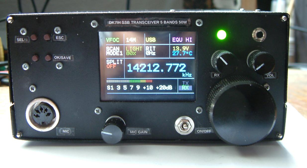
An SSB transceiver for the five “classical” amateur radio bands (3.5, 7, 14, 21 and 28 MHz) will be introduced briefly. It is generally designed as a mobile transceiver for use when parking the car in interesting places. The output power is 50W PEP on all bands with 13V DC power supply. The design involves an ATmega128 microcontroller, a large colored LCD, a DDS controlled VFO, a single conversion superhet receiver with 9MHz interfrequency (IF) and a 5 stage power transmitter equipped with bipolar transistors.
The transceiver is compact, the cabinet expands to the size of 19 x 12 x 7 centimeters. Basically we have a redesign based on the “6 band experimental transceiver” with some alternations in the receiver and transmitter section.
Microcontroller (MCU) board
The MCU in this project is an ATmega128 8-bit RISC controller made by AVR/Microchip. It is clocked by an external crystal at 16MHz. As the display the author has chosen an 8-bit 320×240 pixel color LCD (ILI9341) in parallel mode. Therefore screen display is ultra fast.
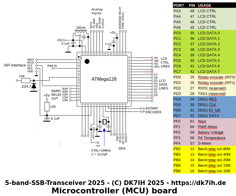
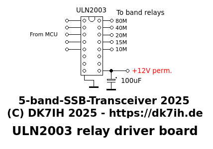
The 5 band relay bus is driven by an ULN2003 driver IC directly controlled by the MCU. This IC uses open collector circuit and also has preinstalled clamp diodes to cope with high inductance voltage generated in the relay’s coil when being switched.
Receiver, SSB signal generator and TX mixer
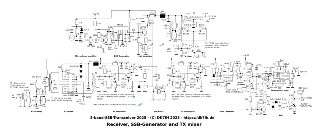
Receiver Description
The receiver is a single conversion superhet with 2 IF amplifiers, AGC and one rf preamplfier stage. On the left we start with the radio frequency amplifier equipped with a dual gate MOSFET (all types can be applied, from historic 40673 to BF991 or its equivalents). The input is connected to the band pass filter set. The main purpose of this stage is to improve S/N ratio on the higher bands but also increasing gain on all bands when band conditions are weak. The stage is AGC controlled to avoid overdrive of the first mixer stage.
The mixer stage uses the SL6440 integrated circuit which has become a problem to purchase on the market in the meanwhile. Therefore a resign using another mixer IC or diode ring mixer has been projected but not realized so far. The main advantage of this IC is its high IMD3, depending on the current that is applied via the 820Ω resistor at PIN11. The 820Ω value in this project has proven to ensure a good compromise between IMD3 behavior and current consumption. The mixer is balanced at the input and output which also helps when trying to achieve maximum performance. The radio frequency transformers’ data can be deduced from the schematic.
We next see two interfrequency amplifiers using cascode circuit. As typical for this sort of amplifier we find the emitter of the second transistor connected to the collector of the first. in “cascade” amplifiers this connection goes from collector of transistor #1 to the base of #2. AGC voltage (based on the audio signal) drives the bases of the two transistors which leads relatively low overall resistance in this part of the circuit. Thus the AGC voltage overall is a little bit lower for the dual gate MOSFET in the first stage which reduces gain to a certain degree. Spoken in practical terms this has not shown to have a significant influence on the receiver’s overall performance (gain).
The two interfrequency amplifiers before and after the SSB filter have got identical layout. The overall gain of this part is around 60 to 70 dB.
The product detector applied is an NE602 or one of its equivalents. This stage provides another some dB of gain and is terminated by an audio frequency low pass filter.
Resulting audio signal is subsequently pre-amplified by a simple audio stage with an bipolar transistor in common emitter mode. The final stage is made up of the TBA820M integrated audio power amplifier which has been used because the distortion rate is significantly lower than with the LM386 IC.
As mentioned before the AGC DC voltage is derived from the level of the audio signal. The first stage in this two transistor designs serves as an audio amplifier followed by a rectifier circuit. Next is the DC driver with 2 outputs. The collector together with together with the 3.3kΩ resistor results in a voltage divider to determine AGC voltage with negative functional output in relation to the audio input signal. The emitter is fed to the ADC4 connector in the MCU.
SSB Generator
The SSB signal circuit starts with an electret microphone and the necessary DC supply which provides about 1.5V DC to the microphone. The microphone gain can be set properly with a 10kΩ variable resistor in the front panel. The connections must be made using shielded audio cable to avoid coupling of radio frequency energy from the antenna.
The double sideband modulator (DSB) uses an IC that can be found in many historic SSB CB radios and is still available on the web, the AN612. Carrier suppression provided by this IC can be experienced in the range of 45 to 50dB. It is set with the potentiometer to minimum carrier voltage. Residual carrier can be observed at the antenna output with about 600mV pp. Compared to the output signal with 50W max. power of 140Vpp. at 50Ω carrier, the carrier suppression is around 47dB.
The filtered DSB signal after having passed the SSB filter then is amplified in a simple stage where a BC547 bipolar transistor enhances the gain to around 12 to 15 dB.
This SSB signal fed into the transmit mixer which in this radio is made of a differential amplifier with an added current source. This resembles to the famous CA3028 IC made by RCA until the 1990s.
Band Pass Filter for RX and TX
The band pass filter for the 5 bands in this radio (3.5, 7, 14, 21 and 28 MHz) is switched with small signal relays:
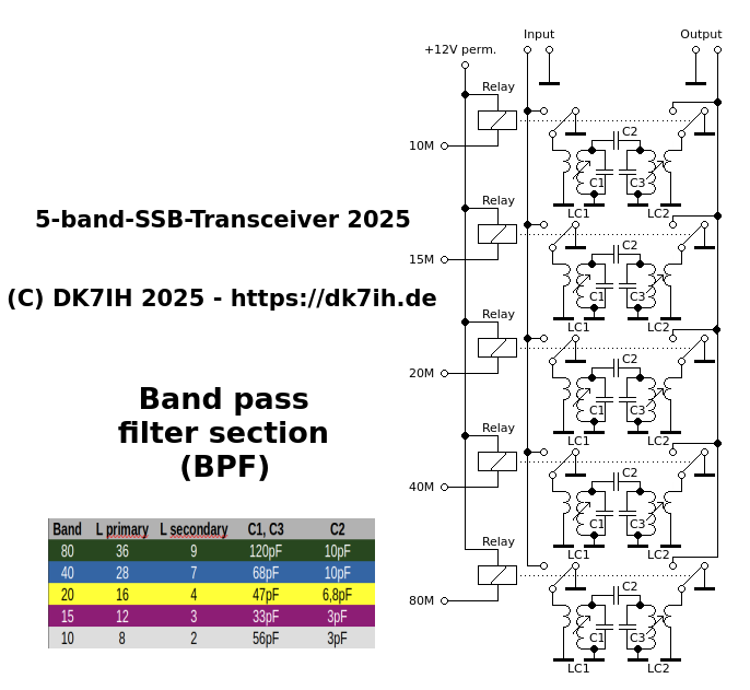
Each set of filters consists of two LC circuits coupled by a capacitor attached to the “hot” ends of each coil. The coils are wound on 5mm TOKO coil formers. The relevant data is given in the table visible in the schematic.
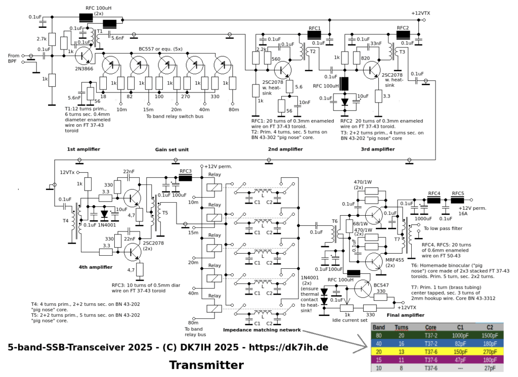
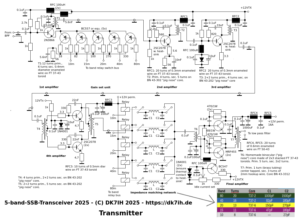
50W Power Transmitter
Following the filter we see the 50W power transmitter circuit.
As broadband power transmitters tend to have different gain on different frequencies in addition the negative feedback loops in each stage a power control stage has been inserted. For each band there is a resistor in the emitter degeneration circuit switched by a single PNP transistor in accordance to the respective band. A good point to start experiments is with 5.6Ω for the 10m band and 120Ω for 80m.
Between the 4th and the 5th amplifier stage an impedance matching network (Pi circuit) has been added. By selecting the capacitors C1 and C2 output and input impedance can be chosen in a wide range to ensure proper matching between the driver and the final stage.
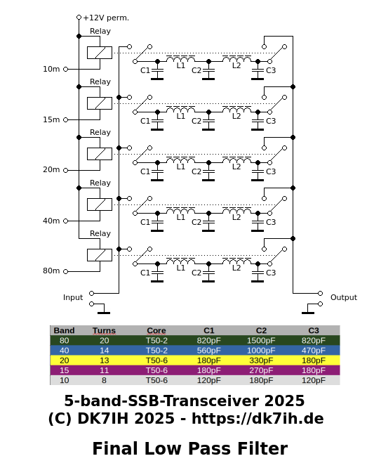
The final Low Pass Filter
This filter unit uses 5 filters for the 5 bands in the radio thus each band can be optimized concerning output and harmonic suppression issues.
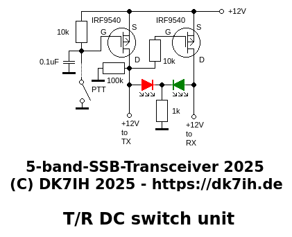
T/R switching unit
To switch between transmit and receive mode my standard circuit has been used. Two power MOSFETs (p-channel) make the switching device:
Practical
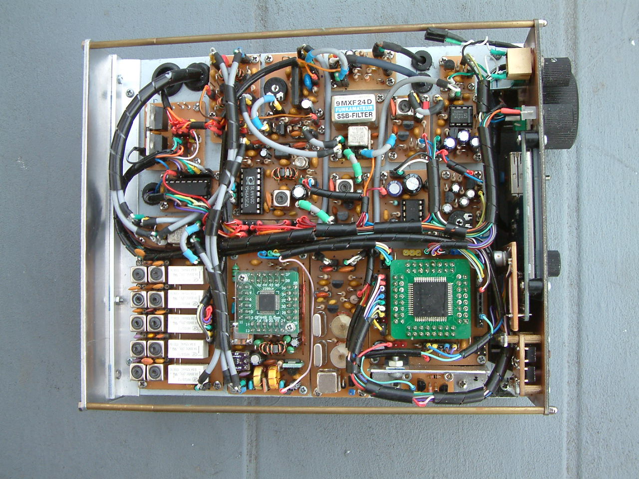
The radio is mounted into the cabinet using two different layers. The first layer makes up the MCU board, the oscillators, the complete receiver, the band pass filter and the T/R switching unit.
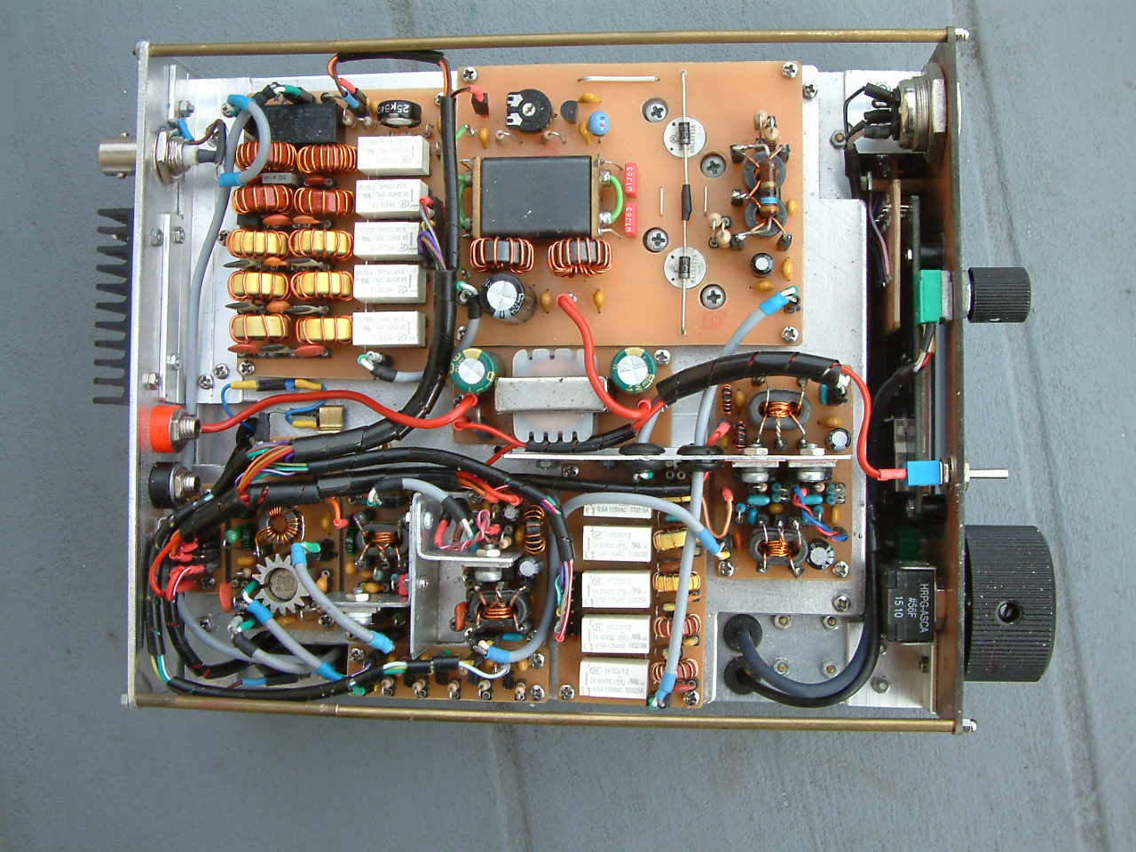
Layer 2 consists of the power transmitter and the final low pass filter:
On the air
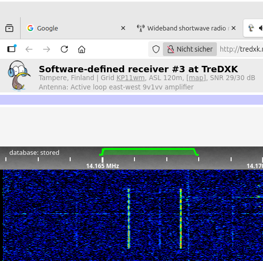
Checked with a Kiwi Web SDR in Finland and a two tone signal, the transceiver can be examined for spectral purity giving the spectrum shown underneath. Output power is 50 Watts PEP on 14MHz
Thank you very much for reading!