Abstract
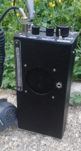
This article describes a portable SSB QRP handheld transceiver with integrated rod antanna (aka “Walkie-Talkies”) for outdoor use. If available a station antenna can also be used. This device is a reliable companion for activities like “SOTA”, hiking, biking are many more. It has been designed for the 20m-Band but can easily be adapted to 17m or higher frequencies. A 12V/2.5amp hours (Ah) battery pack is included which holds enough energy for longer excursions. Another option is to keep the battery pack external in your rucksack an connect it with an appropriate cable. Then the cabinet can be chosen much flatter. 3 centimeters in height is possible in this case. On the picture on the right you can see the version with integrated battery power. With this configuration the complete rig weighs about 500 grams.
Due to the fact that the radio uses a DDS oscillator (AD9835) as main VFO and a ladder filter for SSB generation, the versatile possible combination of VFO and LO frequencies makes it possible to re-design the circuit for other bands, e g. the 18, 21, 24 and 28 MHz amateur frequencies with another DDS (AD9834 based e. g.). This radio has been built and tested by the author for use in the 14- and 18-MHZ band with very good results.
For this radio, a proven and reliable circuit has been chosen. This includes a single conversion superhet receiver, DDS VFO, a crystal controlled local oscillator (LO) and a three stage linear amplifier in the transmitter section capable to supply 5 watts PEP to the antenna. The radio can be used as a “Walkie-Talkie” with in-built rod antenna and external or attached battery pack. It also might be employed as a stationary QRP-transceiver using a (much more effective) base antenna.
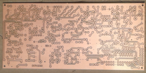
As I have frequently been asked to make PCBs for my radios, here is one. See the related products in my new QRP online shop
Visit DK7IH QRP-Shop
Vy 73 de Peter (DK7IH)
The radio (without externally attached battery pack) can be put into a cabinet of 20 x 9 by 5 cm (7.87″ by 3.54″ by 2″) which should fit into any traveller’s bag, rucksack or what so ever…
This article will describe the assembling process of the complete radio step by step analog to the several functional units sited on the PCB.
General description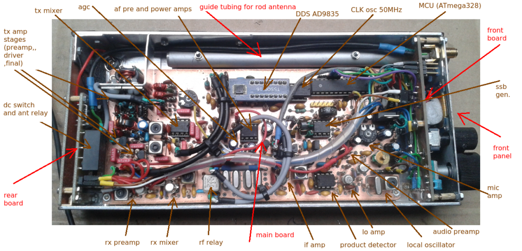

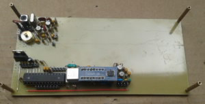
The complete radio consists of 3 printed circuit boards (PCBs):
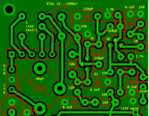
- Main board (containing all circuits for the radio, see picture on the right),
- Front board (holding controls and OLED display),
- Rear board (containing power supply circuits and RX/TX relay).
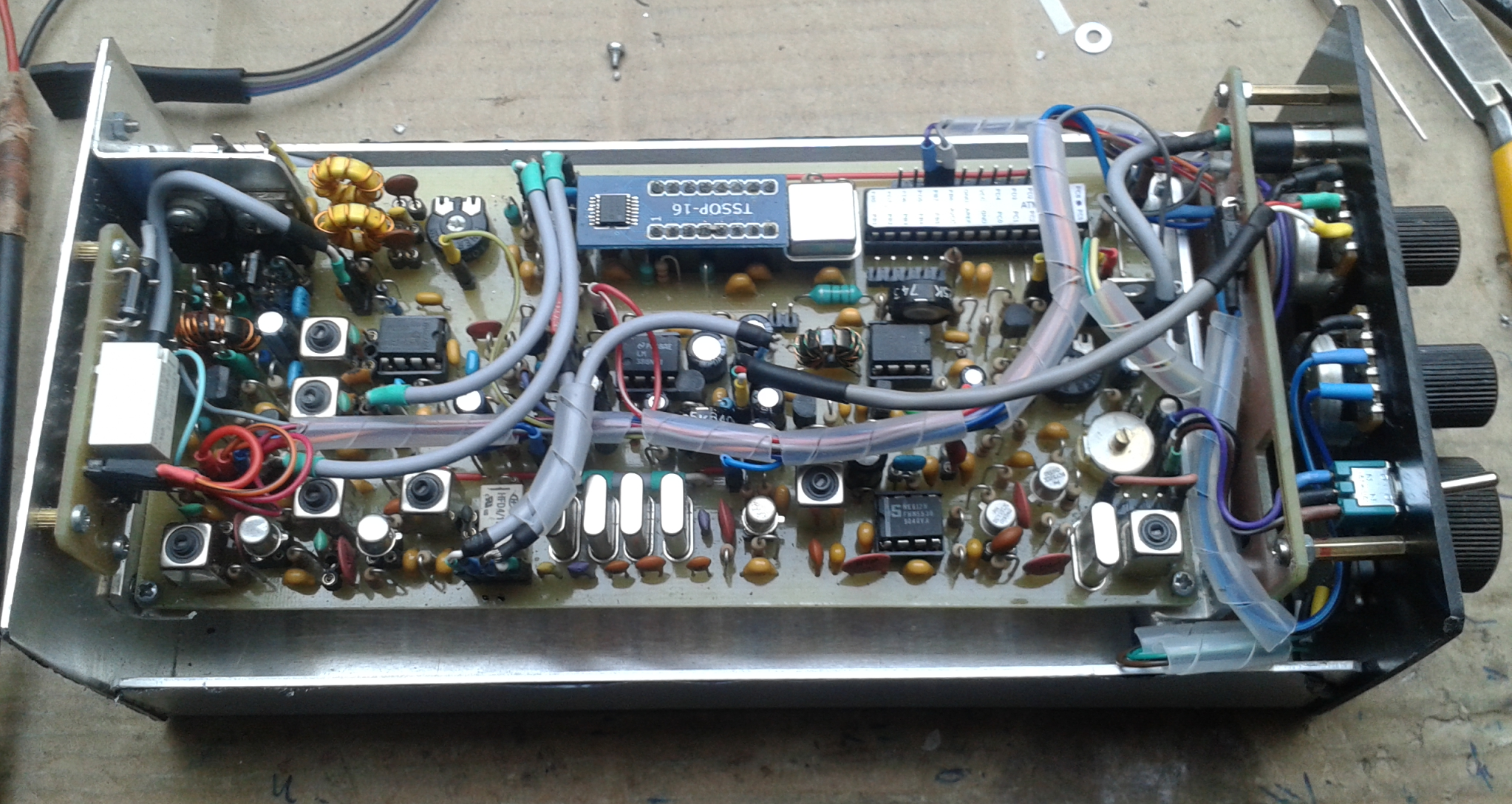
The various functional (i. e. rf related) units of the main circuit are placed on the central board as shown on the right. Please click on the picture to see a high resolution image. Interconnections between the boards are in “old style” technique using simple flexible or shielded cable. We will talk about that later by showing detailed procedures to set up the interconnections. There aren’t that many, if possible they have been placed on the PCB.
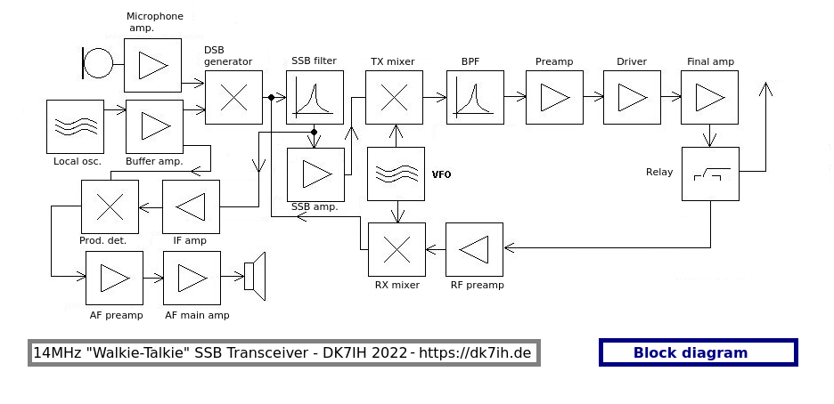
Block diagram
The design of this radio is not really new, we have chosen a rugged standard QRP radio with one interfrequency, SSB-ladder filter (to keep costs low) and a dual-gate MOSFET and some NE612/SA602 as mixers. And some the other “usual suspects”. 😉
VFO and LO
A digital (DDS) VFO is used in this circuit. This ensures absolute frequency stabilty particularly when the radio is used under portable conditions. The respective IC is the AD9835 made by Analog Devices (AD). For amateurs not keen on soldering SMDs I have put the AD9835 on a breakout board. The clock rate for this IC comes from a 50 MHz crystal controlled oscillator for 5V applications. The software runs on an ATmega328 microcontroller unit (MCU). The software is free to download from my Github repo.
An OLED integrated in the front panel shows the current data like frequency, signal strength value of incoming signals, transmitter power etc. Tuning is done using a rotary encoder. The software also holds 16 VFO memories to make operating the radio more comfortable.
Returning to the hardware topic, the VFO is followed by a two-stage amplifier to produce sufficient output level (3 to 4 Vpp. approx.) for the receives mixer stage.
The local oscillator applies a “classical” design (Colpitts circuit). The single crystal used here can be “shifted” above (using a series C) or below (using a series inductor) its nominal frequency to set the LSB and USB frequencies properly. To decouple the oscillator effectively from the succeeding mixer stages a buffer amplifier has been added.
Receiver
This unit is also a standard construction I have used many times before. Two dual-gate MOSFETS used as radio frequency (rf) amplifier in front end stage and receiver mixer coupled by tuned circuits achieve excellent sensitivity, very low noise and high rejection of unwanted signals this together leading to nearly non-existing intermodulation products. The overall gain in the receiver strip is tremendous. It is a “This radio receives with a wet finger”-device. 😉
A ladder-filter made of four crystals (frequency in the range from 8 to 15MHz) is followed by an inter-frequency amplifier that is also equipped with a dual-gate MOSFET. The filter is also used for the transmitter, switching between to applications is performed using a subminiature relay.This amplifier as well as the input amplifier stage are controlled by the voltage generated in the automatic gain control unit (AGC) delivering the ability to withstand even very high input signal levels without running into distortion.
The product detector is an IC SA602 followed by an audio low pass filter, an audio preamplifier stage and the main audio amplifier.
Transmitter
The radio is designed for an electret microphone thus the necessary DC voltage is provided on the audio line. The balanced modulator uses another SA602 mixer circuit. After the DSB signal has passed the SSB-filter it is amplified in a bipolar transistor another SA602 that mixes the SSB signal to the desired output frequency.
The power stages consist of a preamplifier (2SC829, 2SC1674 or equivalent), an 2SC1973 driver and a final stage (2x2SC2078) in push-pull mode. Output power is around 5 watts PEP.
Cabinet
A simple construction has been applied (just as a suggestion). The main frame is made of a piece of u-shaped aluminum (9 cm (3.54 Inches) wide, 3 cm (1.18 Inches) high. The overall length of this U-frame is 20 cm (7.87 Inches). A top cover made of 0.8mm thick aluminum bears the loudspeaker and the earphone jack.
The battery set is not included within this part of the cabinet. A DC socket is mounted by the lower end of the frame to the reverse side. So either a box containing the battery cells can be mounted to the rear of the aluminum frame or the “power pack” can be connected via a DC cable and it can be carried inside the user’s pocket or rucksack.
Building the Radio
We will describe the whole built of the radio step by step (i. e. stage by stage). We will hereby refer to the PCB that is offered for this radio. The building starts with the setup of local oscillator (LO) first, succeeded by the microcontroller and the VFO plus post-DDS amplifier. Then resuming with the receiver, beginning with the two audiostages and then, step by step, moving towards the receiver’s front end. Next is the transmitter, commencing with the microphone am, DSB generator, SSB amplifier, TX mixer and the 3 final stages.
The Receiver
A – The Local Oscillator
The local oscillator provides the signal for producing the double sideband signal (DSB) when transmitting and the signal also used to decode the interfrequency representation of the SSB signal by the the output of the interfrequency amplifier. The circuit consists of two transistors (Q1 as oscillator, Q2 as buffer amplifier):

L is a coil used to trim the oscillator frequency to the exact value needed for the upper sideband generation. Cv, by the way, a 90pF max. trimmer capacitor, does the same for the lower sideband (if desired). Because this radio is designed as a kit, some amateurs might want to use their own crystals. Thus lots of types of crystals and frequencies might be used for the oscillator and the SSB ladder filter, a wide variety of possible conditions of possible crystals have to be covered. This is done by supplying a tapped coil and a 5-pin header strip. By bridging the optimized tap point to the very left pin of the header strip the optimized inductance can be found and set.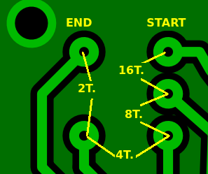
The coil is wound using 0.2mm diameter (No. 32 AWG) enameled copper wire on a 5 mm TOKO coil former. The winding scheme is as shown on the right (viewed from top): From the pin “START” 16 turns are brought onto the coil former, then the next pin (center pin on the right) is covered with 3 or 4 windings on the pin and afterwards soldered. Then the coil setup resumes by winding 8 turns on the next chamber and so on. (Hint: A ready made coil is available on request).
Transistors for Q1 and Q2 can be any NPN type with transition frequency around the desired operating frequency. In tests even AF types like the BC547 could be used without an problems to occur. 2N2222A is recommended instead. Please remind that connection scheme must be E-B-C in this stage!
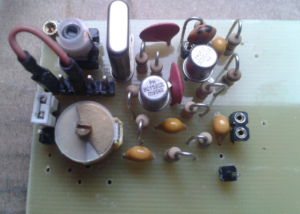
In practical realization the local oscillator looks like shown in the picture on the right. Sideband switching is performed by a standard switch integrated into the front panel and positioned directly in front of the 3 pin header connector (mainly to keep leads short). The center pin of this connector is used only when testing the generator, a standard jumper connector can be used to switch the desired sideband.
The 150pF capacitor connection oscillator and buffer stage can be inserted into a 2-pin header strip (IC socket). This allows variation of the final circuit’s output voltage.
Test and check
The output voltage of the LO depends on the value of the coupling capacitor which is placed between the two stages. With the 150pF capacitor according to schematic it should be around 6Vpp. With a very much smaller value of 24pF it is around 1.5 Vpp. Slight distortion is neglectable.
B – The VFO (DDS AD 9835)
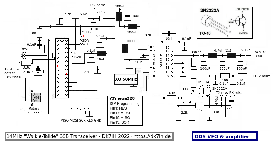
The VFO and its microcontroller (MCU) are the central parts of frequency generation in this radio. The MCU is an ATmega328 (or ATmega168 if you prefer), driving an 132×64 pixel (I²C) OLED. User access is controlled by 3 switches as a simple control interface and a rotary encoder is applied for frequency adjustment.
First let’s have a look to the schematic for the complete VFO section on the right.
Some additional information:
The rotary encoder is soldered to the front panel board to be discussed later. Also a debouncing circuit will be integrated there.
In the buffer amplifier all suitable NPN transistor with “E-B-C” pin configuration can be used. 2N2222A is just to be seen as a suggestion.
Assembling the microcontroller part of the board
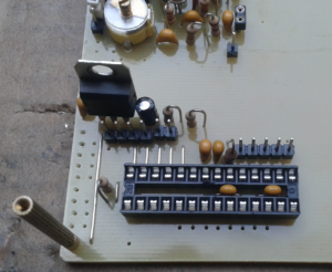
We start with e microcontroller part of the DDS VFO.The number parts for this section is low, they are easily to be soldered to the board. An larger picture can be seen here.
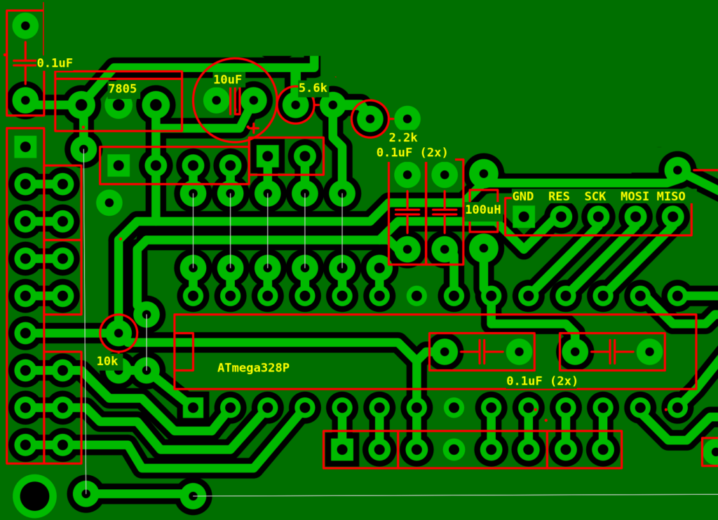
There are some bridges made of uninsulated hookup wire (grey lines in the picture):
- One long on the very left,
- one short at the 10k resistor
- 5 more lines with the ADC inputs of the microcontroller.
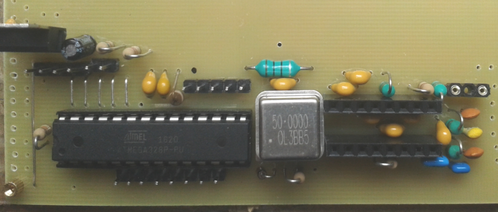
This part of the PCB in assembled state can be seen on the right (click for higher resolution):
More Hints:
- As this is a through-hole design for amateurs not very much acquainted with SMD soldering, the AD9835 has been mounted to a breakout board. This is available in my shop via e-mail (webmaster(at)dk7ih.com) ready to use with AD9835 soldered on it.
- There is a set of socket strips on the left side of the board. These connectors are part of the interface between front board and main board and will be defined later.
Test and check
- Do not insert a microcontroller yet, first check when applying 12V to the “12+ V perm.” connector used for the LO test, if there are 5V present at pin 8 of the ATmega328P.
- Then check if the MCU can communicate with a PC via a programming interface (e. g. the “USB-Tiny AVR programmer“).
For example you can transmit the command
avrdude -c usbtiny -p m328p -U lfuse:w:0xe2:m -U hfuse:w:0xd1:m -U efuse:w:0xff:m
via the interface (in my case I use the “USB tiny”-programmer) to the controller which sets the device to 8MHz clock and prevents EEPROM to be erased after programming.
If all is OK, then proceed to the DDS part of the VFO, if not check for solder bridges and “cold” solder joints.
(To be continued…)
Clock oscillator and DDS
Next part to be soldered to the board is the 50MHz clock oscillator needed for the AD9835 DDS chip. I have put this unit into a socket as well as all the other ICs. Once this component fails (which I had several times the recent years) you can easily dismantle the circuit without the need to unsolder the broken unit and to resolder the new one.
The DDS module AD9835 is an SMD IC in TSSOP16 package. To make building the radio easier I have used a respective breakout board. It has a very slim form factor and can be put into 2 rows of pin headers (8 contacts in each row), right side of the picture:
The assign the components mentioned in the schematic above to the board, here is the detailed layout of this part. Click here to see full size of the layout drawing.
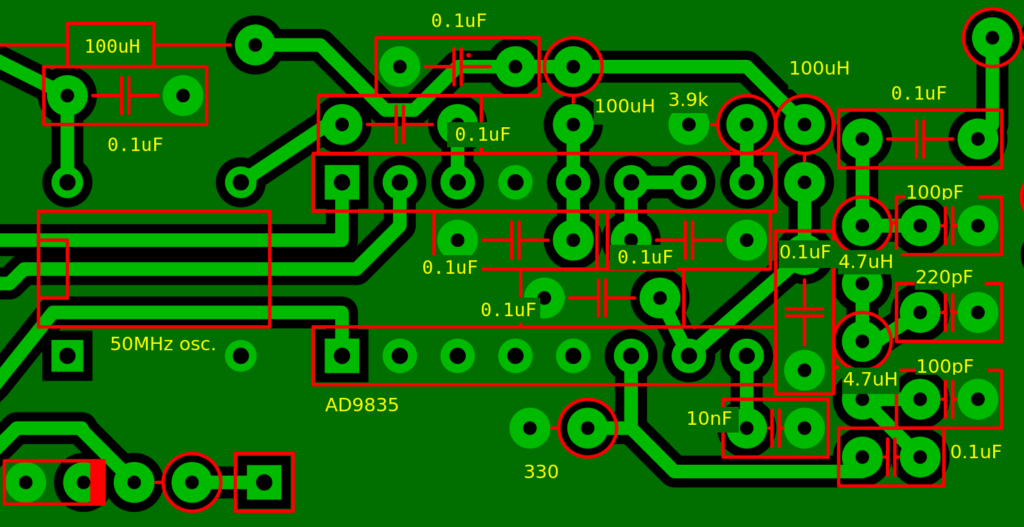
Hint: The 2 pieces of 4.7uH coils are off-the-shelf radio frequency chokes. In spite of their comparatively low Q factor I have used them because they save space and are easy to obtain.
Test and check
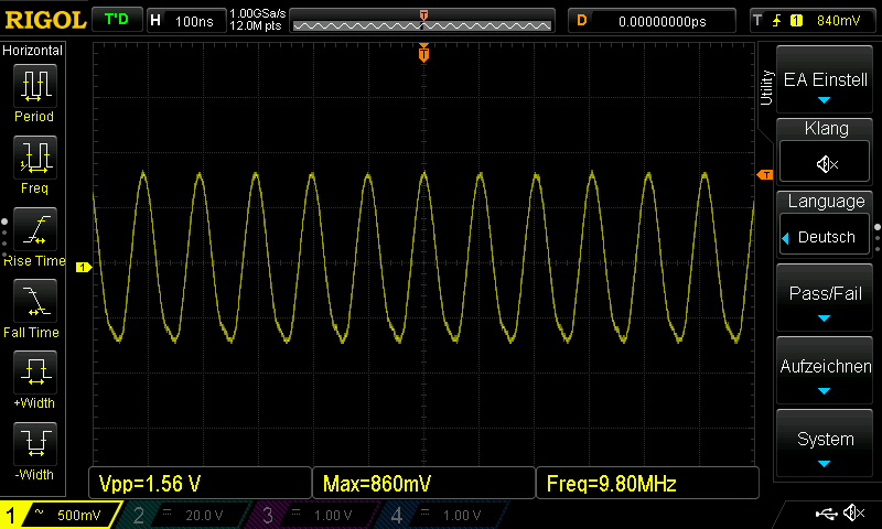
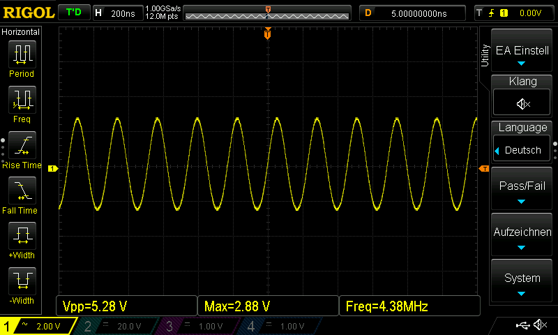
Before you can test, you have to load the software into the microcontroller. There is a so called “HEX-file” on my Github-repo. For uploading this file to the MCU the “AVRdude” software is recommended. If you have problems, do not hesitate to mail: webmaster(at)dk7ih.de!
After the software has been loaded and the microcontroller is re-started, it produces a sine wave with a frequency of about 4.5 MHz. This should be detectable by the 0.1uF capacitor seen in the right top corner of the excerpt above. Voltage is in the range of 0.5V to 0.8V pp.
The post DDS amplifier
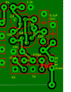
The two-stage linear amplifier is designed to deliver a relatively high output voltage that is mandatory for using a dual-gate MOSFET as a mixer. Dual-gate MOSFETS in this mode require oscillator voltages in the range from 3 to 5Vpp.
With the circuit is in the schematic above, the respective transistors are Q3 and Q4. In this case, as same as with the local oscillator it has already been mentioned, nearly every type of bipolar transistor with the “E-B-C”- pinout can be used. 2N2222A is a good recommendation here.
As Q3 and Q4 are located very close together on the board, keep an eye that, if you use transistors with a metal case, they do not touch!
Rx is basically the 3.3k resistor drawn in the schematic. If you find that the amplifier to put out significant less than 5Vpp. you can lower this value as you need it.
Test and check
Before testing the post DDS one line must be completed. In the picture below you can see a red insulated hookup-wire that is used to power the DDS amp with 12 volts DC.
After that the output voltage of the amplifier should be 5Vpp. approximately with a pure (i. e, undistorted) sine wave form.
With this step, the local oscillator and the DDS VFO have been completed.
Thus, it is time to stick to the receiver, starting with the audio amplifier section.
Building the Receiver
The receiver is a proved and tested construction offering low noise, excellent sensitivity and due to AGC usage is capable of coping even with very strong signals. There are four coils used for interfrequency and receive band signal filtering.
A word on the coils:
All coils are wound on small TOKO (5mm) style coil formers. They have 16 turns primary of 0.2mm diameter (#32 AWG) enameld wire. All coils have this data, no exceptions!. The tuned circuits only vary in the amount of the paralleled capacitors. See the following table to determine the respective paralleled capacitor:
| Frequency | Capacitor in parallel |
| Interfrequency (9 to 11 MHz) | 120pF |
| Receive frequency (14MHz) | 47pF |
| Receive frequency (18MHz) | 33pF |
If you should have difficulties to achieve the TOKO coil former you can purchase a set of 7 ready-to-solder-in coils (1 inductor for the local oscillator (LO), 4 for the receiver and 2 in the transmitter) for 20 EUR/USD from webmaster(at)dk7ih.de + shipping (depending on the country of destination)
Audio amplifier and automatic gain control (AGC)
First the circuit:
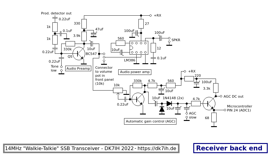
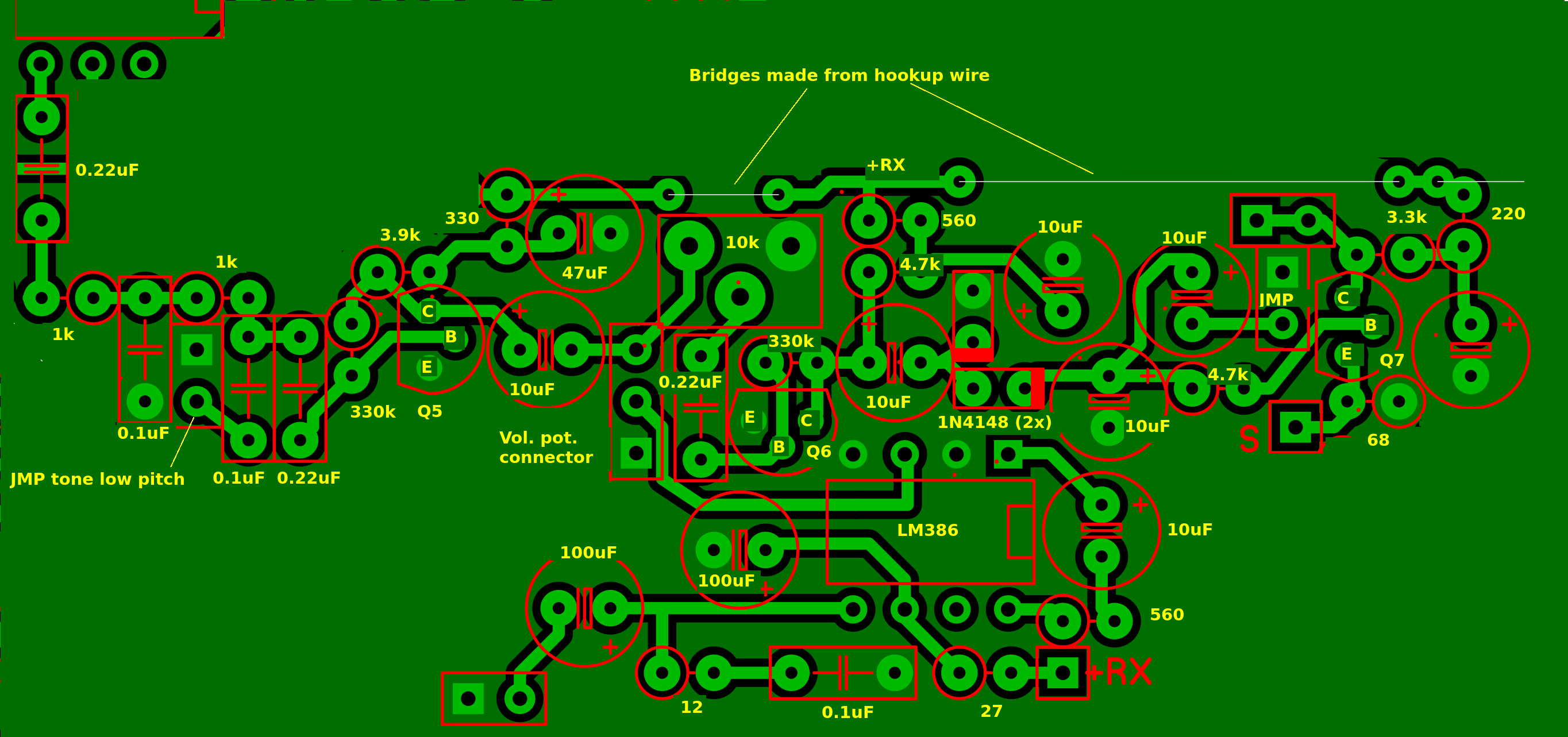
In practical this is the respective part of the PCB (Click for large resolution):
Hints:
There are two jumpers in this part:
- For tone pitch set (bridged jumper adds 0.22uF to the audio low pass filter thus cutting of the higher frequency components in audio spectrum more effectively.
- For AGC delay time extension (some extra Mikrofarads prolong delay hold time, 47uF recommended but this value can be altered to your personal preference!)
Test and check
a) Final audio amp
This test is fairly simple. Connect a loudspeaker to the amp’s output, power up the audio amp (pin “+RX” in the picture), take a metal pair of tweezers or an unsinsulated screw driver and touch the center pin of the 3-pin volume variable resistor connector. A loud hum should be heard from the speaker.
A more sophisticated procedure can be to connect a sine wave generator (f=1000Hz, Voltage about 30 to 50mV pp.) to the input and an 8 Ohm resistor to the output of the stage. With full driving an output power of about 1 Watt should be displayed on an oscilloscope. This means you should read about 8Vpp. on the scope’s screen without much noticeable distortion.
b) Audio preamp
The same test like before. Connect a volume potentiometer to the 3-pin header, put it to center position and perform the test with the input on the audio amp.
c) AGC
Here a sine wave generator is needed. Connected it to the audio preamp, set a frequency of approximately 1000Hz. Connect a DC voltmeter to the “AGC out” pin (in the picture connected to the collector of Q8). Put a sine wave signal (some Millivolts) to the input of the audio preamp and measure DC voltage at AGC out. When reaching some Millivolts of input the DC voltage at the AGC’s output should drop to approximately 0V.
The two audio amps (AGC section not yet completed) on the PCB: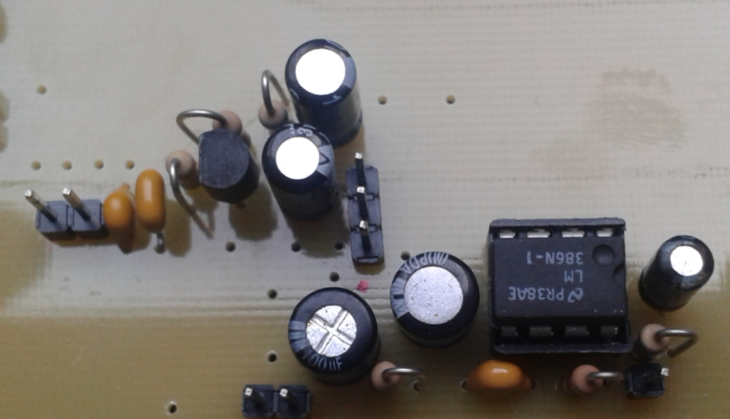
Product detector and interfrequency amplifier
We are heading towards completion of the receiver section. This is the circuit for the product detector and the interfrequency amplifier:
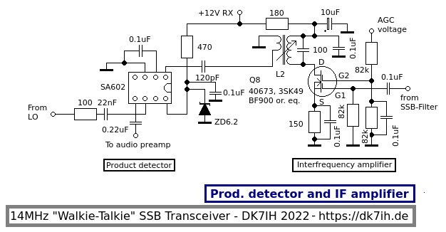
This is also a gain enhancement stage as the NE612/SA602 mixer offers about 12 to 15 dB of gain as well as the singe step dual-gate MOSFET equipped interfrequency amplifier. The last-mentioned also is included in the AGC chain (like the rf preamp sited in the front end).
L2 (together with its parallel C of about 100pF) is a tuned circuit for the desired interfrequency. It is wound on a 5mm TOKO style coil former with 16 turns primary and 4 turns secondary. All coils for the radio are available on request by mailing webmaster(at)dk7ih.de. Complete set of all coils (6 pieces) is 20€/USD + shipping.
The board layout:
Test and check
For testing this unit any oscillator capable producing a weak signal with the interfrequency is suitable. It can be an old-style dip-meter, a signal generator or whatever. Direct connection to the input pin is not necessary. A small “antenna” connected to the generator is sufficient.
Product detector
Switch on the radio in “receive mode” (i. e. audio amp and preamp powered as well as the local oscillator). Some noise must be heard in the loudspeaker. Now turn on the signal generator setting a frequency very close to the interfrequency of the radio. A sine wave tone must be detected.
Interfrequency amplifier
Touch gate 1 of the dual-gate MOSFET with a short piece of insulated wire but do not connect your fingers directly to the gate input to avoid static discharge an destruction of the sensitive device! The capacity of your finger through the insulation material will couple enough radio frequency energy into the circuit to show a result. The tone must heard and should be significant louder than before. Now connect 12 V DC to the AGC input. This must lead to another increase in gain in this stage thus the audio tone must have also a measurable increase in volume.
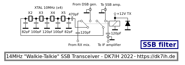
SSB Filter and receiver front end
In this transceiver a ladder filter made of 4 crystals filter is used. Basically the builder can select any interfrequency between 8 and 15 MHz provided that oscillators’ (VFO and LO) frequency or harmonics do not fall into the receiver’s passband in this constellation over the whole tuning range. With some randomly chosen crystals, this filter curve resulted (here setup with 9MHz crystals from a Chinese supplier):
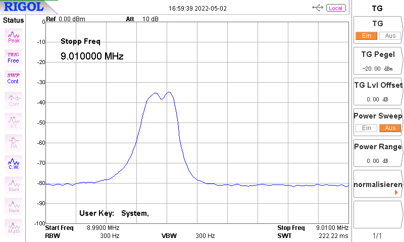
Even if there is a certain ripple on top of the curve, the filter is absolutely usable for a QRP radio.
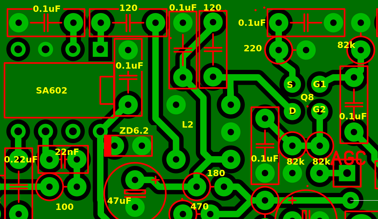
The SSB filter full circuit
This part of the circuit involves the SSB filter made of the 4 crystals, the capacitors and a switch relay because this filter is used for receive and transmit purposes alternately.
The relay is an HFD4/12 subminiature type available for through hole (TH) and SMD soldering. In this unit the TH type has been built in. The relay is connected to the +12V TX power rail thus it is activated when the radio is used in transmit mode.
There are plenty of places for capacitors on the board which sometimes not all have to be used. It is recommended to set up the desired filter on a breadboard first, take measuring data (with a spectrum analyzer an and tracking generator if present) and then transfer this setup to the PCB. On the other hand results with randomly chosen crystals were very much encouraging which later measurements showed. Another idea is to place that capacitors into socket strips and do experiments this way.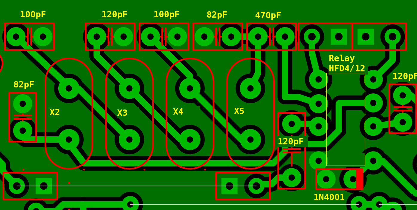
The layout of this specific part of the board:
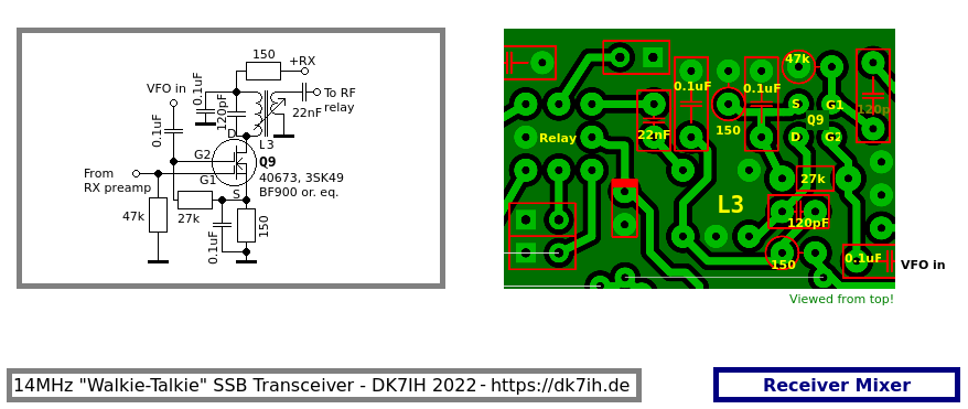
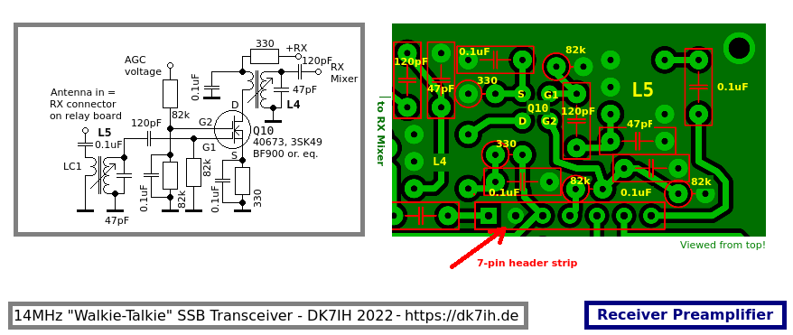
Receiver front end (mixer and rf preamplifier)
These two stages are equipped with dual-gate MOSFETs. It is recommended to mount them in a set of 2 by 2 pins socket strips for easy change, testing etc. If you should have problems buying the through hole like the 40673, 3SK49 or equivalent, you can purchase BF998 SMD types mounted on small breakout boards with webmaster(at)dk7ih.de.
The mixer is very stable towards high level signals and very low in noise production. It requires a comparatively high oscillator voltage of about 3 to 5 Vpp. which the VFO will produce.
The radio frequency (rf) preamp is designed to improve the overall noise figure of the receiver and to make weak signal better discernible against the background noise. It is connected to the AGC chain like the interfrequency amplifier also is.
The RX mixer
The schematic and the board layout:
The RX radio frequency amplifier
Receiver test procedure
Having come to this point, you can test the receiver as a complete device. But before that can be done, some steps must be taken:
Test setup
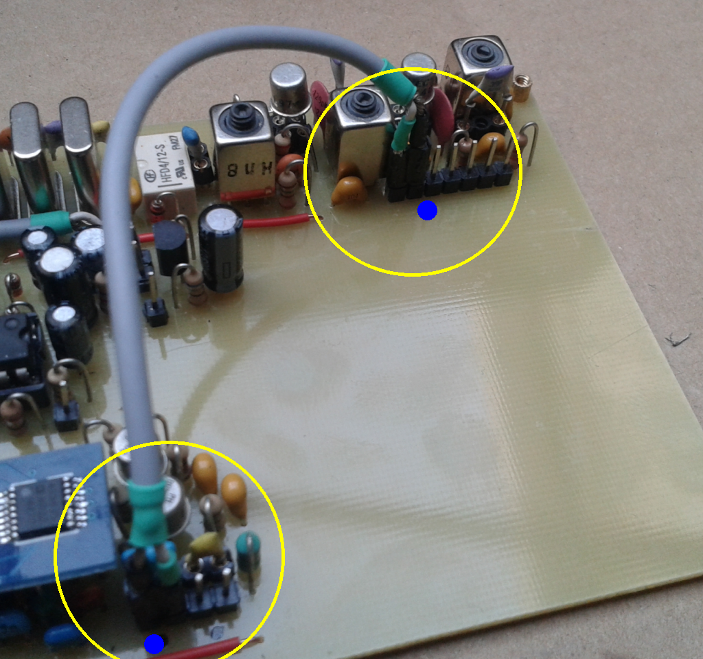
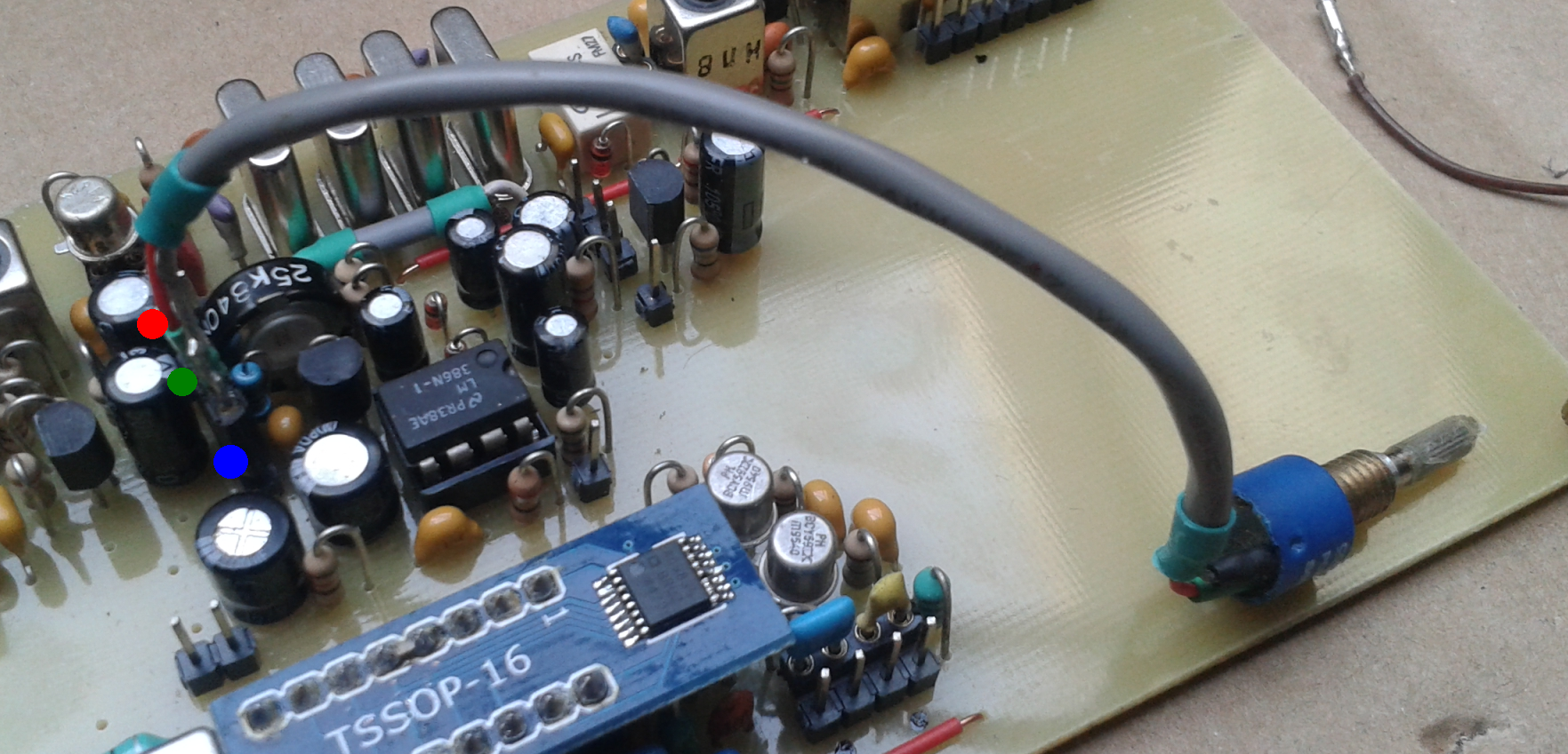
A) Insert and solder (if not yet done) a 7-pine male header strip into the respective place in the rear part of the board. It contains the various DC lines as well as the oscillator input for the VFO and the antenna connector.
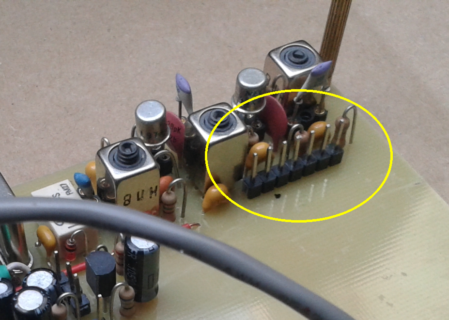
B) Prepare a shielded cable for connecting the VFO amplifier output (left side of the 4-pin header strip) to the VFO input in the rear part of the receiver section (pin 1 and 2 in the long header strip, counted from the left). Note the position of the shield connector marked by blue dots!)
C) Connect a variable resistor (aka “potentiometer”) to the 3 pin in the center part of the audio amplifier. Not that the GND pin of the potentiometer is marked in blue, the center pin in green and the 2nd outer pin in red.
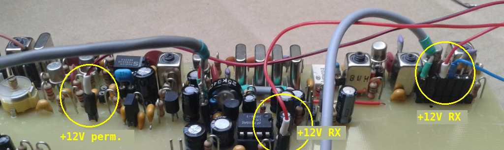
D) Connect the DC lines. Hint: Here we find 2 types of 12V rails:
- 12 V permanent (for the oscillators, i. e. the very left connector)
- 12 V RX for the receiver only.
For testing they will be connected together to the 12 V supply rail. Using a current limited supply (or at least a 100mA fuse) is recommended. Later these leads will be separated again and will be connected to the respective pin on the relay board positioned in the rear section.
E) Connect the AGC output and the inputs:
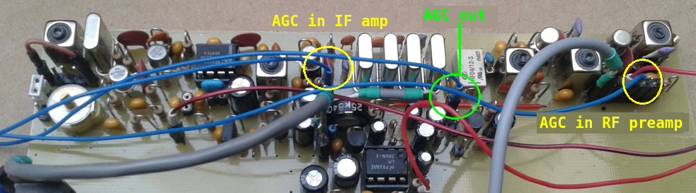
All 3 lines are soldered to a common potential for testing. Later, when finally installing them, an rx gain set potentiometer will we installed to the front panel. Wiring scheme will be explained later!
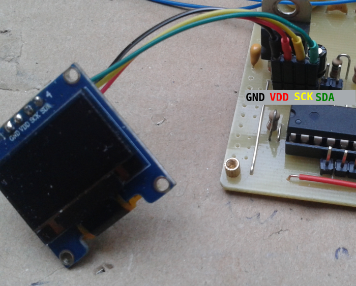
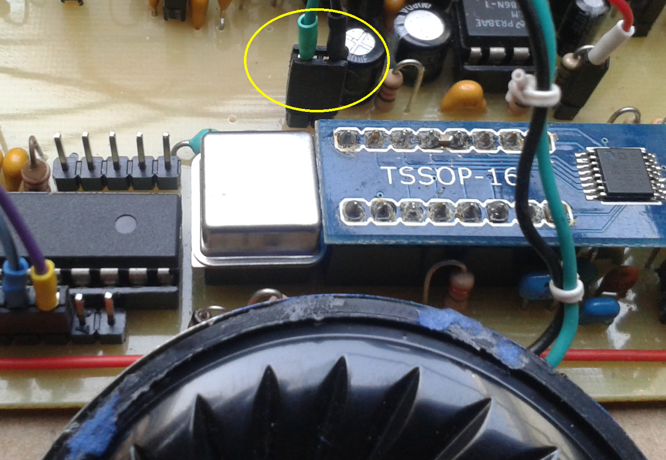
F) Connect an I²C OLED display to the 4 pin header close to the microcontroller:
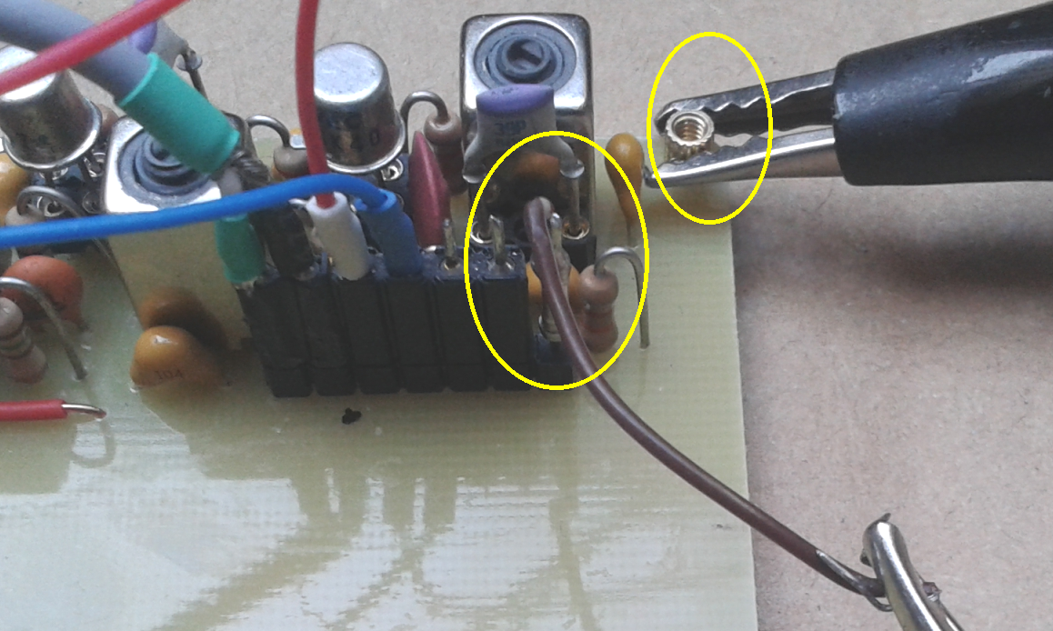
G) Connect a rotary encoder to the front header strip:
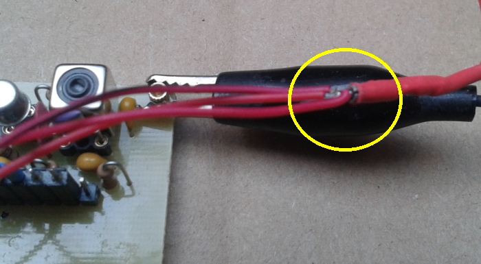
H) The antenna must be hooked to the very left pin of the header (brown cable), the cable’s shield goes to a bolt inserted to the corner hole:
I) Supply 12V DC to the respective VDD lines. Be sure not to forget the GND (aka “minus”)!
J) A loudspeaker also must be added:
Performing receiver test
With all the prerequisites met we can start testing the receiver. Make sure to have software (HEX-file) uploaded to the microcontroller. After powering on the circuit, the typical band noise must be heard in the loudspeaker, the display should show “14.200” kHz. If you wish to build the radio for another band, please mail to webmaster(at)dk7ih.de.
Now tune the 4 coils (counted from the right) to the maximum signal gain achievable. Now tune into a station on the band. If the pitch is unnatural or the sideband is false then set the local oscillator respectively:
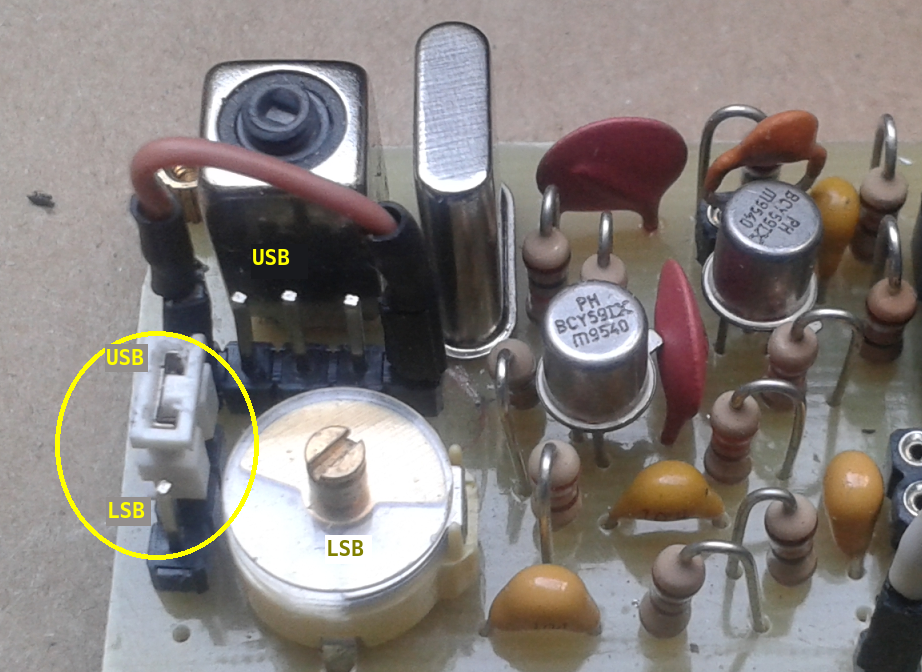
To change the pitch of the received signal in USB mode select another connector of the 4 right pins close to the coil and hook it to the very left pin and tune the coil to achieve natural sounding band noise. This last-menzioned pin always is fixed because it marks the end of the tapped coil. To set LSB (if required) just turn the trimmer capacitor slight amount of an angle.
After all settings have been made correctly, the receiver should sound like this:
Now having completed (hopefully successfully!) this test the receiver is ready to go. If you should encounter problems, please drop me a mail (webmaster(at)dk7ih.de).
The Transmitter
The transmitter section of this project starts with the microphone amplifier and the double-sideband generator (DSB generator).
Microphone amplifier ans DSB generator
The radio is designed to be used with an electret microphone. Even if taken into account that an electret microphone offers high output voltage due to an integrated one-stage field-effect- transistor (FET) equipped amplifier (which sometimes delivers enough output voltage to drive the SA602 balanced mixer directly), we have integrated an audio amplifier into this circuit. QSOing is easier if you don’t have to scream into the microphone. 😉
The next step that follows is a balanced modulator (DSB generator) with an SA602 as central part. A simple way to optimize carrier suppression has also been integrated.
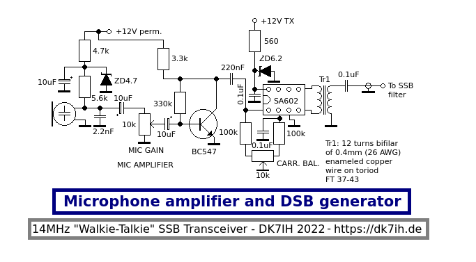
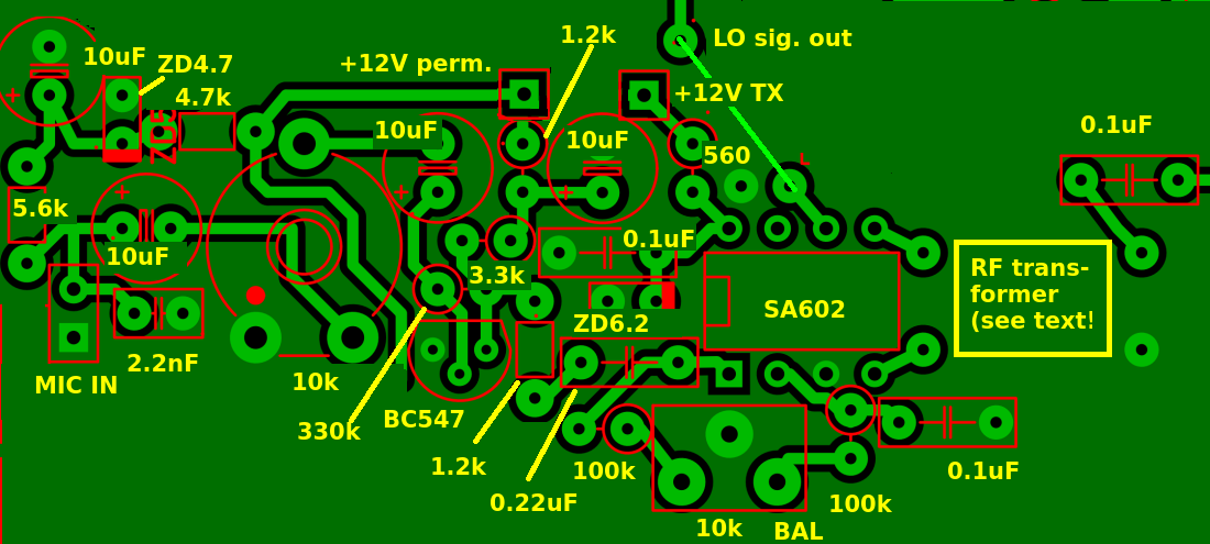
On the printed circuit board (PCB) this section starts on the very left side of the board, vertically in the middle of the scope:
This stage is terminated by a radio frequency transformer. The data is 12 turns of 0.4mm diameter (26 AWG) enameled wire using bifilar winding. This circuit takes advantage of the two symmetric outputs of the SA602 thus enhancing output voltage significantly. The secondary of this transformer is connected using shielded cable with the TX connectors of the relay switching the SSB filter either to receive or transmit mode.
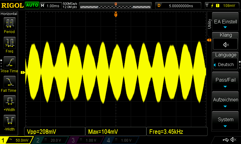
A sine wave or, even better, a dual tone oscillator is requires for this test. Put bout 20mV of audio signal to the microphone input and watch the signal after it has passed the SSB filter. The resulting voltage should be about 200mVpp at the filter output.
SSB amplifier and TX mixer
The post-SSB-filter amplifier is a low gain stage. Its only purpose is to shift the SSB signal up to 3 to 6 dB to ensure proper driving of the TX mixer stage. Then the TX mixer follows. The signal is fed into a band pass filter consisting of two tuned LC circuits for the desired output band.
The schematic:
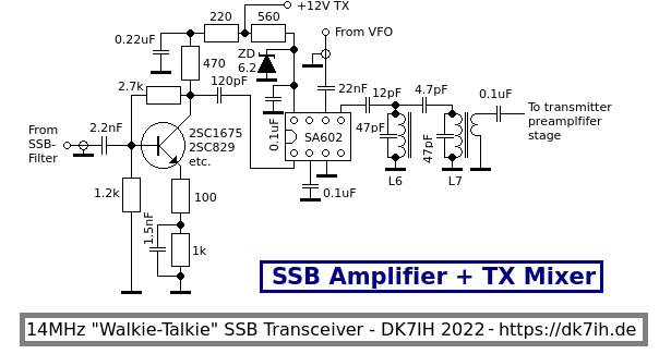
L6 and L7 are the same coils that have been used in the receiver section: 16 turns primary, 4 turns secondary on a 5mm TOKO style coil former.
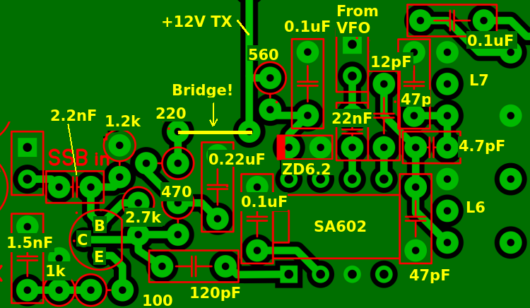
Here is the board layout with the respective components:
Test and check
As before a dual-tone generator is used. The signal that appears by the output of the SSB amplifier should be in the range of 750mVpp. to 1Vpp. when fully driven.
The signal by the end of the of the transmitter mixer’s band pass filter should be in the range of 500mVpp. L6 and L7 must be tuned to maximum output.
(To be continued tomorrow, so stay tuned! 🙂 )
Final RF amplifier
This section will complete the main PCB. We have e three-stage amplifier section made from bipolar transistors. The first and the second stage are in A-mode, the final push-pull amplifier is configured for AB-mode. Final output power is around 5 Watts PEP. The circuit:
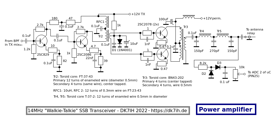
Hints and tips:
- RF transistors are a suggestion. The can either be pulled from old CB gear or be ordered in my shop. Please ask mailing to webmaster(at)dk7ih.de.
- The 2SC2086 should be equipped with a heat if possible. Test runs have shown that, on the other hand, it can stand several hours of uninterrupted “on” status without any problems. The 39kOhm resistor can be replaced by the value of 47ohms without losing significant power.
- D1 should be thermally connected to the the 2 final transistors.
- Output power measurement is done with the microcontroller (PIN25 / ADC2)
- “TX out” is connected using a shield cable, preferably with 50Ohm impedance.
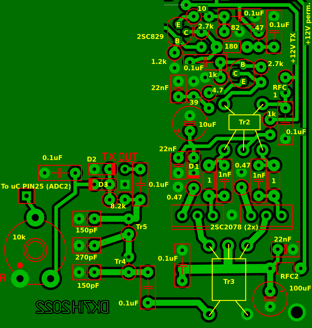
The respective board layout:
Test and check
Before testing the final amplifier, check that the board is ready for testing (Click for full sized image!)
![]()
Put a temporary heatsink insulated to the final transistors’ cases. This will be replaced by a permanent heatsink later.
Connect lines +12V permanent and +12V TX to the respective connectors on the header strip in the right side of the PCB. The pins are assigned as demonstrated underneath: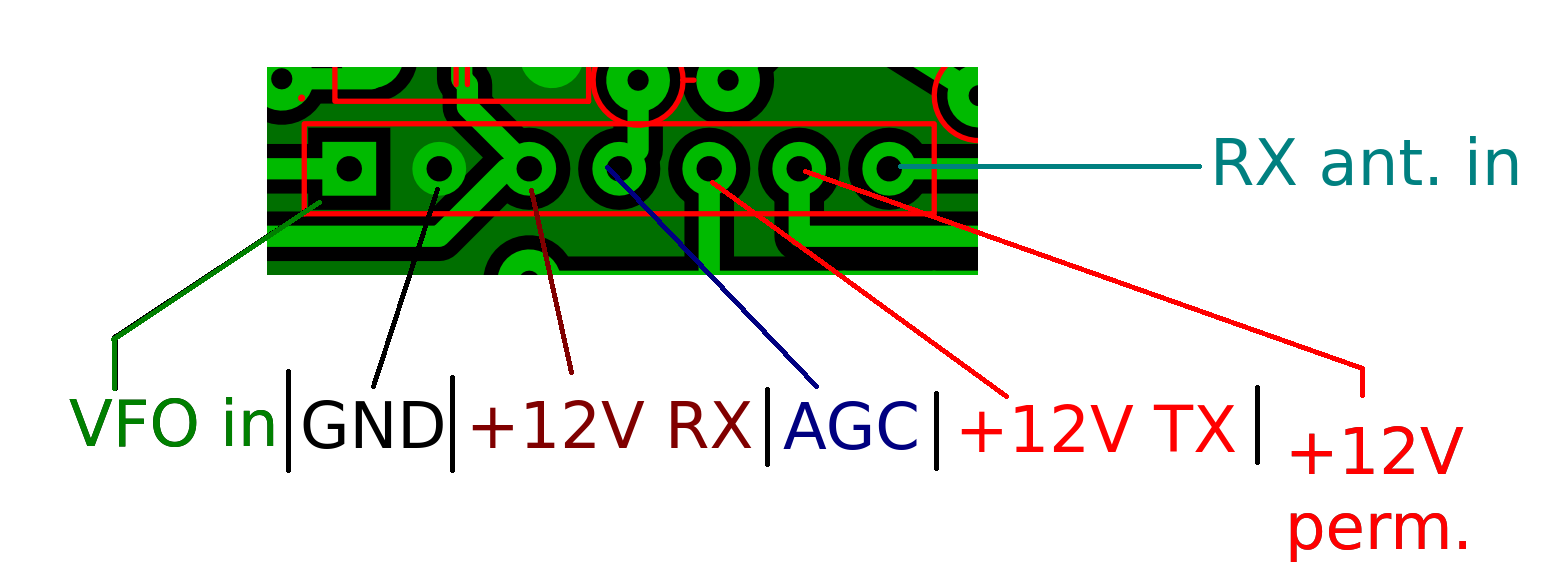 Now follow these steps:
- Take an ohmmeter and measure the collectors of the two final transistors against the heatsink. Some hundred ohms or more should be read on the meter depending if the heatsink is connected to GND or not. If “0 Ohms” occur, check the insulation of the transistors to the aluminum heatsink.
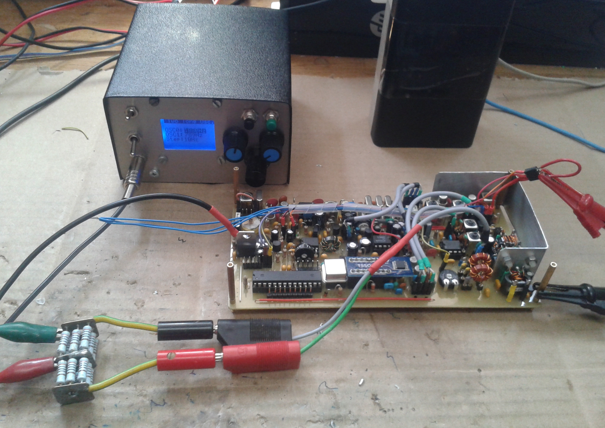
- Connect a 50Ω dummy load to pin “TX out”.
- Connect the oscilloscope to the dummy load.
- Connect a two-tone-generator to the microphone input on the left side of the PCB.
- Switch lines +12V permanent and +12V TX to a 12V power supply with a current limiter integrated. At least a 500mA fuse should be present.
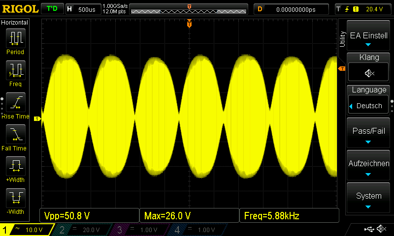
On the scope you should see the typical waveform of a two-tone-signal applied. Output voltage should be in the range between 43 and 45 Vpp. which equivalents to about 5 watts output PEP.
Transmitter test setup:
Output on dummy load:
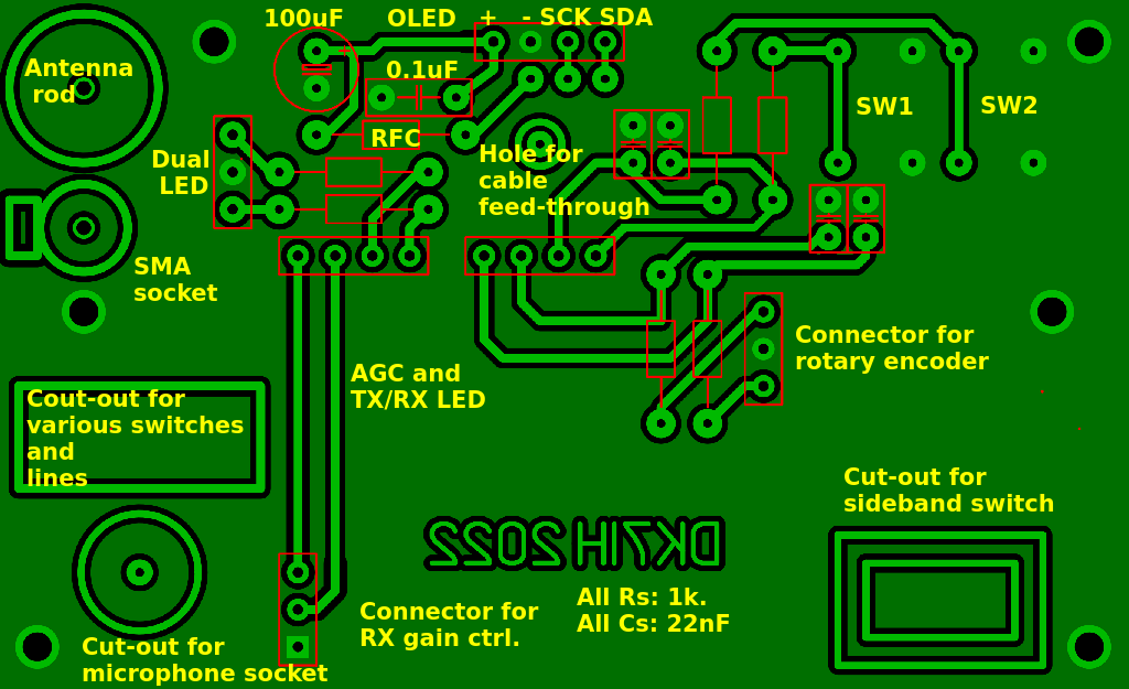
The Front PCB
Some controls are placed on this, some are not. This has been done to allow the QRPer to use as much of his own components as possible withou being forced to buy certain specific parts. Let’s have a look to the layout first:
Hints:
- The OLED is an 1.3″ display with an SH1106 type controller. Other OLEDs also can be used (SSD1306) but this requires a minor change in software. Also keep an eye on the polarity of VDD (+) and VSS (GND). For some types of OLEDs they might be reversed. For all OLED types PCBs are available, so no confusion should occur. Please ask if you have any question on this topic: peter(at)dk7ih.de
- The cut-outs are made to put the lines through an use connectors elsewhere on the board.
- The switches are standard mini push-buttons.
The assembled front board:
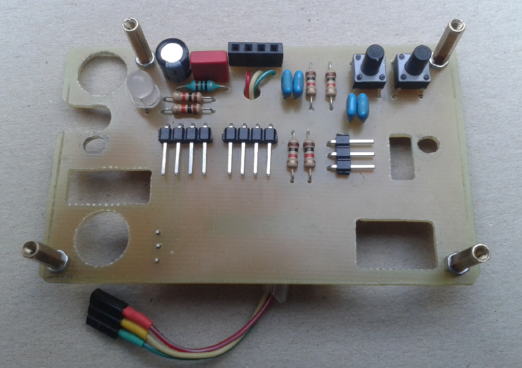
Hints:
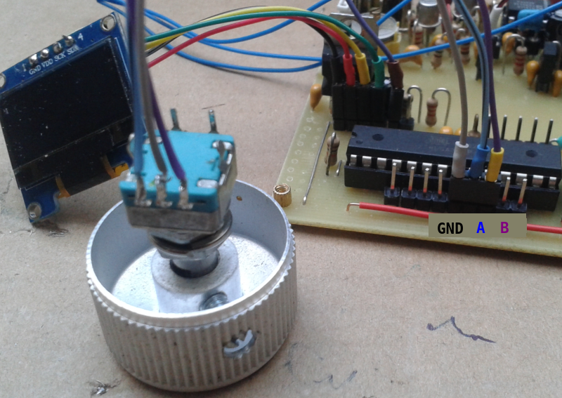
- The 3 pins in the left bottom corner are for the RX gain control potentiometer that is connected on the back of the board.
- Center right you can see a 3-pin connector for the rotary encoder. This rotary encoder only has the connectors “A” and “B” but no additional switch.
- Spacers are “M2” sized and must be fit individually in length so that the front cover fits to the construction:
- The 3 lines (red, yellow, green) connect the OLED. They represent: VDD, SCK and SDA (in that order)
- The audio volume potentiometer should be connected using shielded audio cable to avoid incoupling of stray energy emitted by the OLED. For this purpose pulled soundcard cables from old computers are best because the have two audio lines inside the shield.
- The SMA jack for connecting the antenna (whatever you might use) is directly mounted into the front cover plate.
Integrated into the rest of the assembly, the front panel can be equipped with a plastic front cover. A template for this cover is available on request (peter(at)dk7ih.de). Then all is assembled into the U-shaped bottom part of the cabinet:
For first tests 2 RF lines have to be installed to test the radio:
- #1: From the “TX antenna” port on the rear PCB to the “TX out” connector on the mainboard (in the photo the grey shielded line close to the RF power transistors)
- #2: A shielded 50Ω cable guiding from the “ANT out” connector on the the rear board to the SMA jack in the front cover.
Stay tuned… 🙂
73 de Peter (DK7IH)