by Peter Baier (DK7IH)
Abstract
This unit will cover the basic usage of the Analog-Digital-Converter (ADC) in the STM32F4 MCU. We will develop a simple procedure to read multiple ADC values from various input pins and have these data ready for further processing.
ADC in STM32F4 in brief
The Analog-Digital-Converter in the STM32F4 MCU uses the basic principles of function like most ADCs in other digital circuits: The process of successive approximation. An internal generator (a Digital-Analog-Converter) produces a variable DC signal with different voltage and this is compared to the input signal in a way that in the end the voltages of the two sources (internal DC and external signal voltage) match, so they are equal. By reading the respective DAC data we get the digital equivalent of the externally applied voltage. This process involves a certain time (thus defining a sampling rate) and varies in bit width of the detecting process.
In contrast to AVRs, where the ADC usually has 10bits width, the ADC in the STM32F4 unit can be switched to a maximum of 12 bits processing width. There are up to 3 different ADCs in one MCU depending on the exact model you have in use. They are numbered as “ADC1”, “ADC2” and “ADC3”, if present. They can be connected to certain input pins but not all combinations are possible.
Setting up the ADC
As always to start with a functional unit, this unit inside the MCU has to be configured before we can use it. First we have to have the reference manual at hand. The “ADC”-section starts with page 388. The registers can be found beginning from page 415. Lets directly stick to that part because from the vast set of possibilities to make use of the ADC we will select a really simple approach to avoid confusion.
Some general annotations before we start:
You as a developer can assign certain pins to certain ADC. But not all combinations are possible as mentioned before. They are limited as shown in the following table:
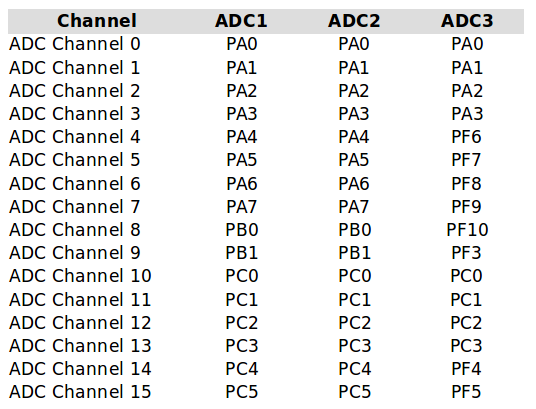
This table is deduced from an entry in datasheet, the “Pinouts and pin description” section table starting on page 50. You can learn how a given input pin can be assigned to a certain ADC channel.In the “additional functions” sections you can see the pins assignable to certain ADC channels.
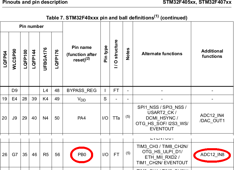
For ADC1 we, to start in in simple way into this more or less complex field, want to use pin PB0 as an input for analog voltage. From the config table above we deduce that PB0 can either be assigned to ADC1 or ADC2 as input channel #8. We will use ADC1. The further steps of configuration are:
//Port config
RCC->AHB1ENR |= RCC_AHB1ENR_GPIOBEN; //Power up PORTB
GPIOB->MODER |= (3 << (0 << 1)); //Set PB0 to analog mode
As you can see PB0 is switched to analog mode which requires writing 0b11 to the respective bits in MODER register.
Next the ADC will have to be set up:
//ADC config sequence
RCC->APB2ENR |= (1 << 8); //Enable ADC1 clock (Bit8)
ADC1->CR1 &= ~(1 << 8); //SCAN mode disabled (Bit8)
ADC1->CR1 &= ~(3 << 24); //12bit resolution (Bit24,25 0b00)
ADC1->SQR1 |= (1 << 20); //Set number of conversions projected (L[3:0] 0b0001) -> 1 conversion
ADC1->SQR3 &= ~(0x3FFFFFFF); //Clear whole 1st 30bits in register
ADC1->SQR3 |= (0b01 << 3); //1st conversion in regular sequence: SQ1: PB0 as ADC1_IN8
ADC1->CR2 &= ~(1 << 1); //Single conversion
ADC1->CR2 &= ~(1 << 11); //Right alignment of data bits bit12....bit0
ADC1->SMPR2 |= (7 << 0); //Sampling rate 480 cycles. 16MHz bus clock for ADC. 1/16MHz = 62.5ns. 480*62.5ns=30us
ADC1->CR2 |= (1 << 0); //Switch on ADC1
The first 3 lines switch the ADC clock signal to “on” (thus power the ADC, disables scan mode which means that the ADC will not automatically run thru the configured channels and do (unnecessary) conversion for our simple example and we set the resolution to the maximum of 12 bits.
Steps from #4 (“Set number of conversions…“) and beyond have to be explained in a more detailed way:
In the STM32F4 ADC the signals to be used for conversions of analog signals are organized in so called “sequences”. There are “regular” and “injected” sequences (we are about to define a “regular” one) and they can contain up to 16 different inputs served sequentially. So, a “chain” must contain at least 1 and may contain 16 channels max.
How many channels are held in a sequence is defined in the SQR1 register (“sequence register”) , namely in bits 23:20:
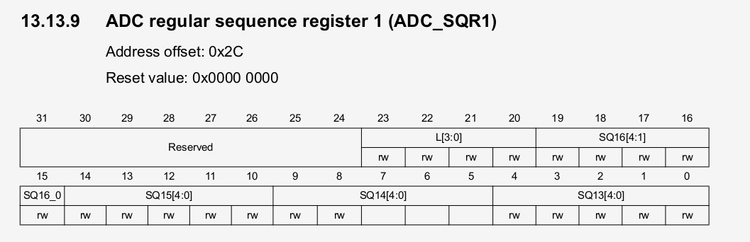
Because we only want to read one input by one time, we write decimal “1” into this set of bits:
ADC1->SQR1 |= (1 << 20);
The next step is to fix what channel will be used (first, if you have more). The sequence to be processed is defined beginning with SQR3, SQR2 and the remaining bits of SQR1 register. As we only have conversion channel projected we directly got to SQR3 register:
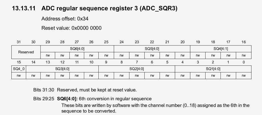
Here bits 4:0 (SQ1) define the first (and in our example only) channel to be read.
ADC1->SQR3 |= (0b01 << 3);
As we want to use channel 8 we shift 0b01 by 3 bits to the left. Another possible (maybe even better) notation would have been “0b01000”. This says that channel 8 will be assigned as first (and int this case only) channel to be processed.
The remaining 4 lines of code define the way of conversion (we perform only a single conversion when called), define adjustment of the data bits (right alignment, so we don’t have to care about actual number of bits appearing after the conversion) we set a sampling rate and, last but not least, we switch on the ADC. Please refer to the reference manual to make clear what these bits are intended for in the respective register!
With this sequence of defintiions the ADC now is “ready to use”.
To read an analog value from PB0 the ADC’s “DR” (data register) has to be read. First we start a conversion by writing the value of “1” into bit 30 of ADC->CR2 register and then get the corresponding digital value from the “DR” register.
uint16_t adcval = 0;
ADC1->CR2 |= (1 << 30); //Start 1st conversion SWSTART
while(!(ADC1->SR & (1 << 1))); //Wait until conversion is complete
adcval = ADC1->DR; //Read value from register
Using multiple input pins
In case you wish to extend this example to, let’s say, two different input pins this can be easily done. You have to redefine the start of the sequence (actually we only have one channel to read, so there is no “sequence”). Let’s say we want to read channel 8 AND channel 9 (PB0 and PB1) of port B.
First: Don’t forget to set PB1 as previously done with PB0 by the begin of the initialization sequence:
GPIOB->MODER |= (3 << (1 << 1)); //Set PB1 to analog mode
Then, before reading a a channel we must reset the respective “begin” of the sequence in SQR3 register. For PB0 we have shown it before, for PB1 it is slightly different:
ADC1->SQR3 = (0b01001); //Set 1st conversion in regular sequence: SQ1: PB1 as ADC1_IN9
After that you can again read the ADC, this time connected to PB9.
Hint: Please note the the usual “|=” operator frequently used for register definition does not apply here! This is because if you try to reset the bits by simply “or-ing” them, their total value will remain unchanged in this case. If you have multiple bits and want to redefine only some of them, first use the “&= ~” operator to reset the bits you are about to modify.
Example code
On my Github repo you can find two files. One to demonstrate the reading of the internal temperature sensor, the second one to show the usage of PB0 as analog input like discussed before. For this example a 4×20 LCD module has been connected to the MCU to give you a detailed reading of data.
Thanks for today an c u!
73 de Peter (DK7IH)