by Peter Baier (DK7IH)
Abstract
In this article we will discuss pulse width modulation (PWM), how the respective signals are produced and how we can use them to control motor, light bulbs, LEDs etc.
PWM in short
When current consuming devices like motors, light bulbs, LEDs etc. have to be controlled concerning their intensity you can either control the voltage driving the device (using Ohms law) or you can control the energy transmitted per time unit that powers the device. PWM uses the latter possibility.
PWM takes advantage of square waves, continously “flipping” between two extreme values: Max. power and zero power. The longer the time power is transferred (compared to the time slice where no power is transferred, the greater the total energy coming to the connected device will be:
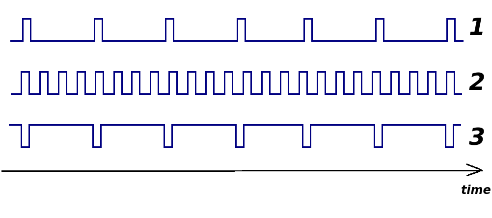
You can see three different waveforms with different so called duty cycles. No. 1 features relative low “on” time and a very much larger time span “off”. Thus the total amount of energy transferred to the connected device is fairly low. No. 2 has about 50% on- vs. off-time each and no. 3 has a large amount of “on” time and relative low time “off”. In the latter case energy brought to the load is higher than in the other two examples.
One advantage of this method is that the driving circuit dissipates very much lower amounts of thermal energy because its resistance is nearly equal to zero when switched and very high when not conducting. Thus, according to Ohms law and power calculation (P = V x I in DC circuits), the amount of thermal energy produced by the semiconductor is minimized.
Usually for practical applications you can not connect the load directly to the microcontroller because it an output port is not capable of driving more than some milliamps. Deduced from this fact one or more driver stages have to be involved. We will talk about this issue later.
PWM generation in the STM32F4
PWM in an MCU is generated by using a timer. This is the ideal tool because PWM has got a lot of things in common with timing as you can see from the graph above.
To achieve our goal we first have to perform a setup sequence for a timer if we intend using it for PWM. In the following example we will use timer 3 (TIM3) in the STM32 MCU device to drive output port PA6 with an adjustable waveform between 0 and 100% duty cycle.
//////////////////////////////////////////
//Setup TIMER3 for PWM control
//////////////////////////////////////////
RCC->AHB1ENR |= (1 << 0); //Enable GPIOA clock
GPIOA->MODER |= (0x02 << 12); //Set PA6 to AF mode
GPIOA->AFR[0] |= (0b0010 << 24); //Choose Timer3 as AF2 for Pin PA6 LED
RCC->APB1ENR |= (1 << 1); //Enable TIM3 clock (Bit1)
Enabling the respective GPIO port (here “A”), setting PA6 to “alternate function” (AF) mode, setting PA6 as AF mapped to TIM3 are the first things to be done. Here the procedure is the same as described before. Check out the “alternate function” table in datasheet starting from p. 62, check out the device you want to have the application for (TIM3 in this case the 3rd column in that table) and check out the port that is going to be used:
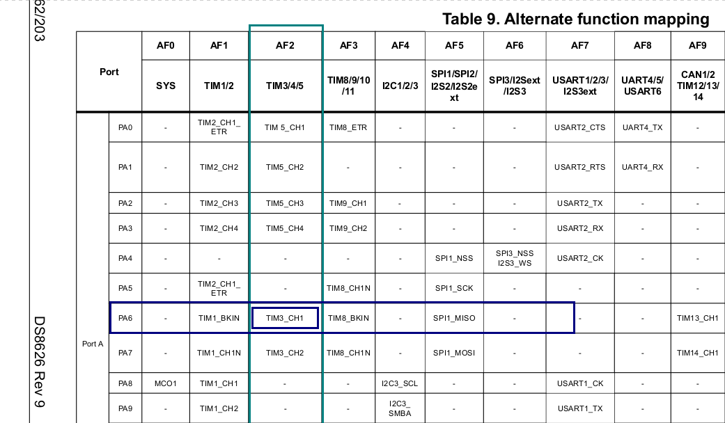
As we intend to use PA6 we have to select AFRL6 in “alternate function” register AFRL which is named in CMSIS as AFR[0]. Don’t get confused, register names are sometimes not matching data sheet or reference manual by 100%!
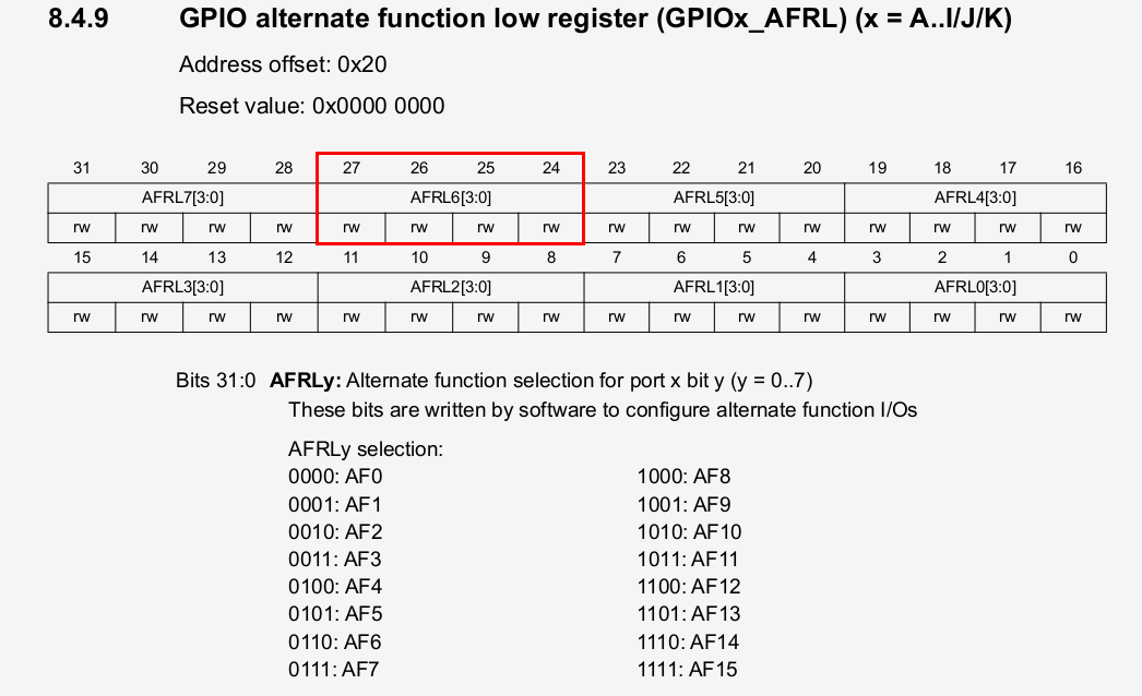
(Source: STM32F4 reference manual p. 285)
The last line of our code example above switches TIM3 clock to “on” so we can use it later.
The next 4 lines refer to the timer settings which have to be defined:
TIM3->PSC = 499; //fCK_PSC / (PSC[15:0] + 1) -> 50 Mhz / (499 + 1) = 100 khz timer clock speed
TIM3->ARR = MAXPERIOD; //Set period max. value
TIM3->CCR1 = duty_cycle;; //Set duty cycle
TIM3->CCMR1 |= (0x06 << 4); //Set OC1 mode as PWM (0b110 (0x06) in Bits 6:4)
First we set the prescaler that is deduced from system clock speed. In the example SYSCLK is set to 100MHz. To learn how to set SYSCLK please refer to unit 3. The prescaler determines the clock rate the counter counts up (or down if you use a downcounter). The respective formula is given in the comment line.
The next register is the ARR (auto reload register) register that sets the “ceiling” the counter will count to before it will be reset. We use 255 as max. value.
In CCR1 register a value is preloaded that sets the initial setting of the timer. That is the value the timer starts to count with. Here we use it to define the current duty cycle.
With CCMR1 we set the timer “output compare” mode:
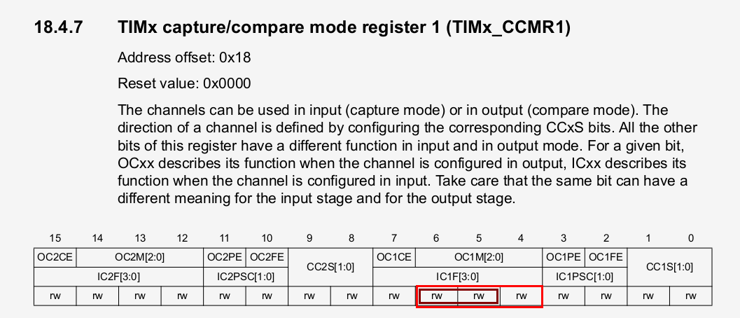
By writing 0b110 (dec. 6) we define “110”: “PWM mode 1” for this counter.
The next block of instructions defines compare mode and interrupt status:
TIM3->CCMR1 |= (1 << 3); //Enable OC1 preload (Bit3)
TIM3->CCER |= (1 << 0); //Enable capture/compare CH1 output
(TIM3->DIER |= (1 << 0); //Enable update interrupt)
First instruction OC1PE: sets “Output compare 1 preload enable” in CCMR1 enabling us to use the preload register.
Second instruction hands the signal out on the corresponding output pin.
Last instruction (in parenthesis) enables triggering the interrupt when TIM6 or 7 are used. Here, with TIM3, this is not necessary.
By the end of the setup sequence we have to activate interrupt usage and activate TIM3.
NVIC_SetPriority(TIM3_IRQn, 2); // Priority level 2
NVIC_EnableIRQ(TIM3_IRQn); //Enable TIM3 IRQ via NVIC
TIM3->CR1 |= (1 << 0); //Switch on TIM3
As always the handler function has to be defined and declared correctly. If you compile using “C++” option you must declare/define the function as extern”C” to get the correct idnetifier of the handler function. The only use of this function is to clear interrupt status after timer overflow has occurred and interrupt has been fired.
//////////////////////////////////
// TIM3 INT Handler (PWM)       //
//////////////////////////////////
extern "C" void TIM3_IRQHandler(void)
{
    //Clear interrupt status
    if((TIM3->DIER & 0x01) && (TIM3->SR & 0x01))
    {
        TIM3->SR &= ~(1U << 0);
    }
}
Setting the duty cycle
Setting the desired duty cycle depends on the driver stage you are about to use, i. e. inverting vs. non-inverting. You can either try:
TIM3->CCR1 = duty_cycle; //Set duty cycle
or
TIM3->CCR1 = 255 - duty_cycle; //Set duty cycle
A word about driver stages
As we pointed out before, you can not connect most loads directly to the output pins. A driver stage is mandatory in this case. These stages can be realized either by using bipolar or field effect transistors. Or you can use integrated circuits. Some examples can be found just by using a search engine.
If you intend using a MOSFET driver it is important to keep in mind that with most power MOSFETs gate voltage must be very much higher than the 3.3 Volts you can expect from the MCU’s output port to drive the semiconductor adequately. In these cases you can use a “low voltage” MOSFET specially intended for these purposes or you can switch in an intermediate driver stage equipped with a bipolar transistor. This is due to the fact that bipolar transistors are current driven wheres MOSFETs are voltage driven. The bipolar semiconductor will switch with a base current around some microamperes and then switch the voltage of the MOSFET gate provided the voltage in your application is high enough.
So, that’s all for today. See you later and “thanks for watching”!
73 de Peter (DK7IH)