Abstract
This article shows a very compact PA module for an SSB transceiver. It has been designed for my favorite band (i. e. 14MHz) but works also fine for 18MHz and 21MHz. With some adaptions it should also be usable on the lower bands as well. A PCB is available in my QRP shop.
The fully equipped PCB:
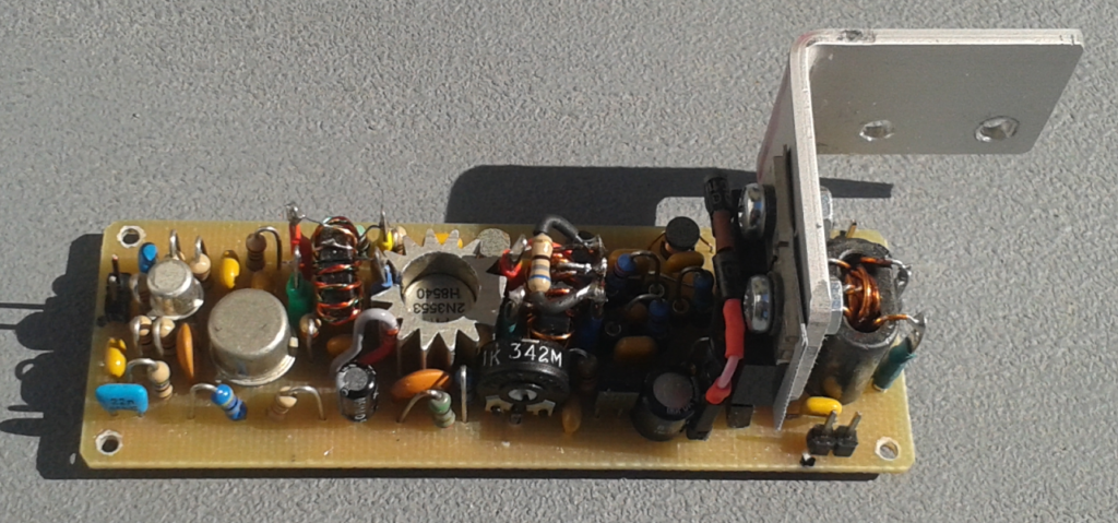
This module is a 4-stage based development equipped with bipolar transistors. It is capable of delivering 10W PEP maximum output with good linear performance. The board size 9 by 3 cm (3,5 by 1,2 Inches).
The Schematic
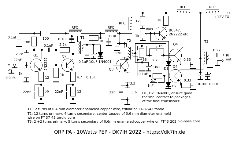
For this module I have used some well-known bipolar transistors:
- Q1: 2N2222
- Q2: 2N2219
- Q3: 2N3866
- Q4, Q5: 2SC2078
Q4 and Q5 can be purchased with eleflow.com or from my QRP webshop.
The two resistors attached to the primary and secondary winding of T2 are subject to experimental optimization. Their purpose is to prevent self-oscillation in this high-gain amplifier. If the resistor connected to the secondary of T2 should be needed, it must be soldered directly to the terminals of the transformer.
Description
The first 2 stages of the PA amplify the input signal (that can be in the range between 100 and 300 mVpp.) to about 150 to 180mW PEP. They are biased in A-mode.
Q3 then is biased in AB-mode by generating bias voltage via an 1kΩ resistor and a 1N4001 silicon diode connected to GND. This diode is placed on the board very close to the heatsink of Q3 to ensure excellent thermal contact. It stabilizes base current by the fact that it will enhance conductivity as soon as Q3 heats up thus limiting the bias current accordingly. So, thermal runaway of this stage is effectively prevented.
Q4 and Q5 are a push-pull final stage. Here 2 regulating diodes are used. Thus a current control stage with an NPN transistor (BC547, 2N2222 or equivalent) has been added. The packages of the transistor also should have good thermal contact to the diodes.
Between stage 2 and 3 and stage 3 and 4 impedance transformers have been added. Their purpose is to reduce the high er output impedance of the previous stage to the very much lower impedance of the succeeding input. The last transformer (T3) works vice versa: The about 10 to 12Ω output of the push-pull amplifier are transformed to 50Ω of the antenna circuit. This circuit will require a low-pass filter that has not been placed on this board because the PA module is designed for various bands. Even usage in a multiband transceiver is possible which requires a set of LPFs on a separate board.
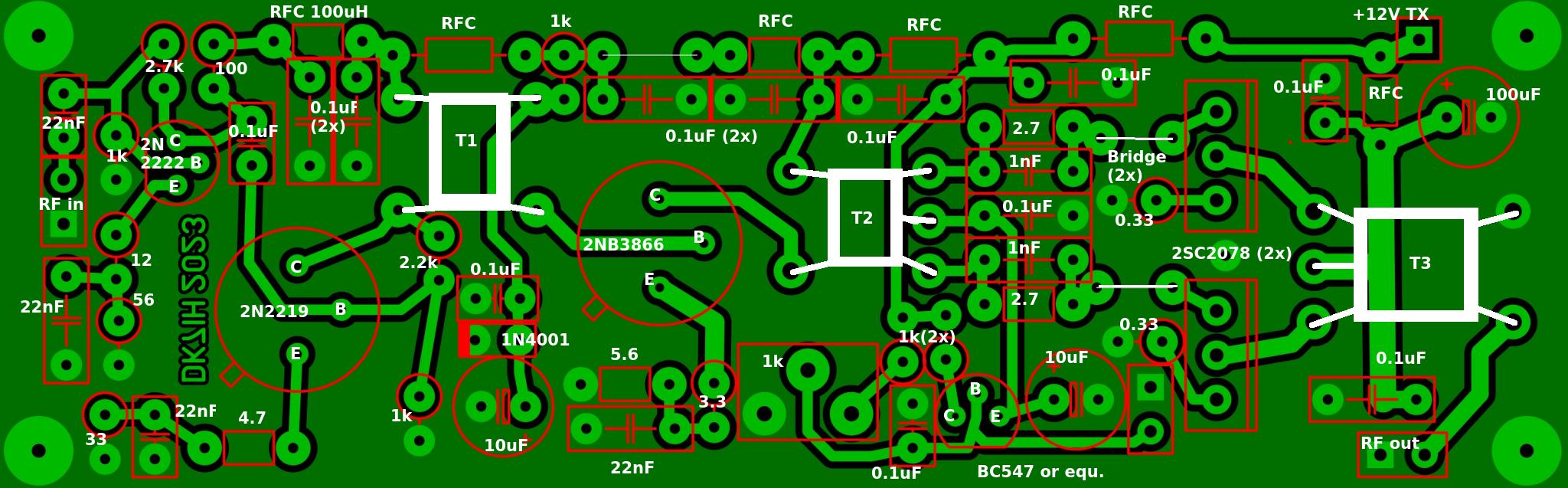
Board layout
The components’ placement on the PCB:
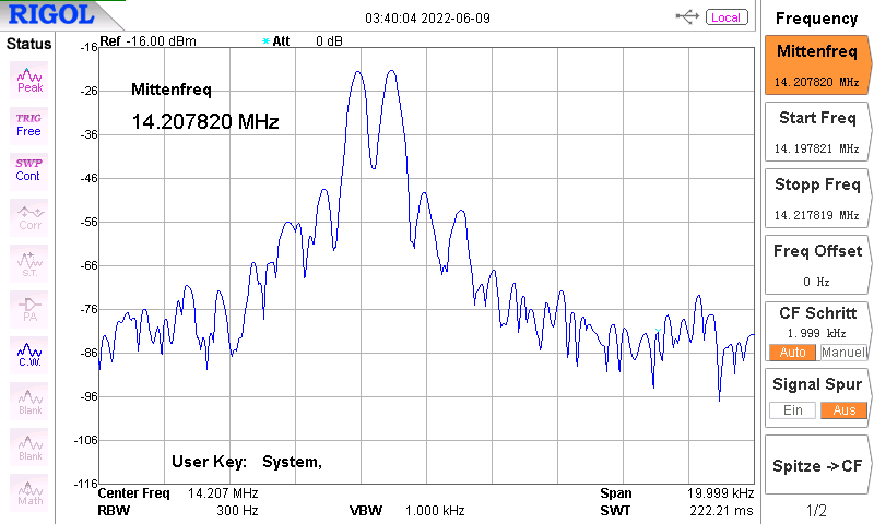
Performance
When driven by a 14MHz SSB signal modulated with a two-tone oscillator we get the following reading on a spectrum analyzer. IMD3 is about 30dB which is acceptable for a QRP PA circuit.