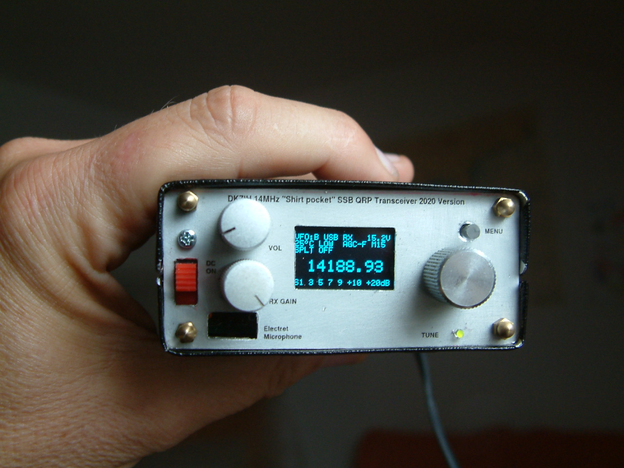
When the project of building a very small transceiver was accomplished 4 years ago, I still lacked lots of skills in setting up electronic circuits using SMD technology. The radio’s craftmanship had been more or less defective to a certain degree (there were still lots of things to learn when using SMDs on Veroboards), the inside looked comparatively “messy” and the performance was not sited within the premium league. Particularly the receiver was prone to IMD (NE612 as 1st mixer) problems when signals on the band were strong. But because I liked the outer appearance of the radio a total revision of the inside had to be performed.
The major changes that were used to improve the radio are:
- Usage of a Si5351 clock oscillator as VFO and LO instead of an Xtal controlled LO and AD9835 as VFO,
- Only one SSB filter (off-the-shelf made) instead of 2 ladder filters,
- Dual-Gate MOSFET as 1st mixer (instead of SA612),
- 2SC2078 as push-pull pair in the final TX stage,
- All SMD components are now mounted to the underside of the board,
- TBA820M instead of bipolar equipped push-pull audio amplifier,
- Cabinet size has been enlarged slightly (about plus 0.5 cm in length),
- Proper cabling instead of “spaghetti” arrangement,
- Copper band has been used to improve radio frequency grounding.
Things that were not changed are frequency layout (14 MHz), the ATMega328P microcontroller (MCU) and cabinet size etc.
Even if the changes to the previous version are minor, I had to revise the schematic nearly completely (High resolution schematic):
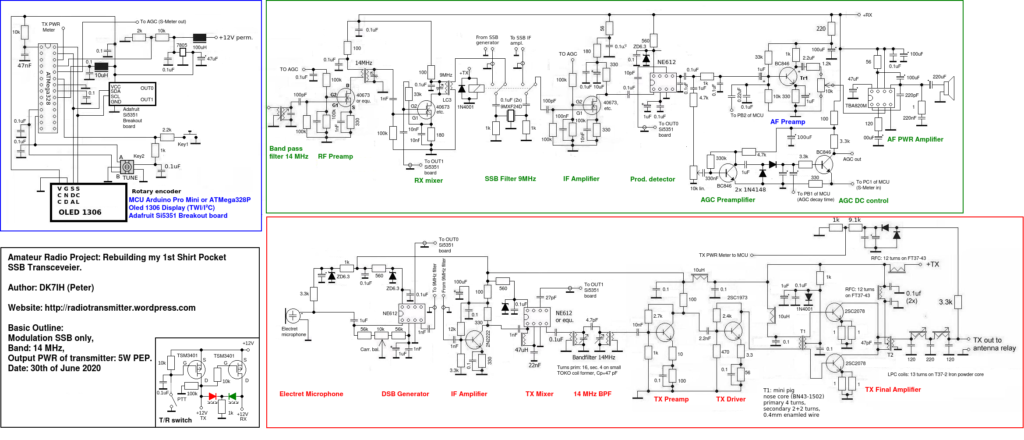
The radio consists of 3 sections:
- Control unit (MCU, Si5351 oscillator, 1306 OLED and related stuff
- Receiver
- Transmitter
Receiver improvements
In the receiver I changed the NE612 into a dual gate MOSFET mixer stage because I found out that the IMD3 was causing problems in the evenings when high signal levels were present. The dual gate MOSFET mixer turned out to be much more stable in respect to high signal levels. With the Si5351 being able to produce about 3 Vpp. of rf energy the mixer could be fed with an appropriate signal level. Dual gate MOSFETS work best when injected signal is between 3 and 5 Vp..
The MC1350 in the IF amplifier had been removed because the simplicity of the AGC hat to be improved. This is is because only one type of AGC voltage had to be produced. The dual gate MOSFET and the MC1350 have reverse AGC characteristics, thus an AGC that controls both types of amplifiers has to produce two types of AGC voltage. One voltage increasing and the other decreasing when signal levels rise in the receiver.
Transmitter improvements
The microphone amplifier was not necessary because an electret microphone outputs enough audio frequency voltage to drive the NE612 mixer directly. An intermediate amplifier with bipolar transistor amplifies between the SSB filter and the TX mixer pushes the signal to an appropriate level, thus enough energy always is present in the first transmitter stages.
The remaining transmitter has been not changed, only the final amplifier transistors have been replaced with a pair of 2SC2078 (2SC1957 in previous version). Transmit power is now 6 watts (when DC is 13.2 volts from my QRP battery package).
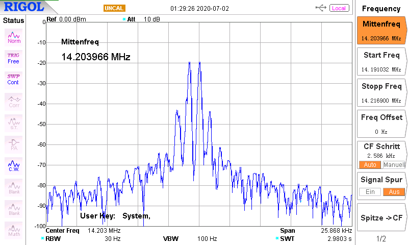
Output spectrum is as follows (Pout = 5W PEP)
T/R switch
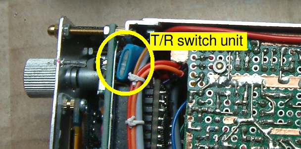
Based on a discussion with WA2MZE here on my blog I tried to minimize physical expansions of a P-channel MOSFET based T/R switch. The basic design can be found here, only two P-channel switching MOSFETs are used.
The circuit is so simple, it fits on a piece of Veroboard just 1 square centimeter in size and put into a piece of heat shrink tubing. After connected to the 12V system it was stored behind the front panel:
The inside has also been straightened (please, don’t say its is still messy! 😉 ):
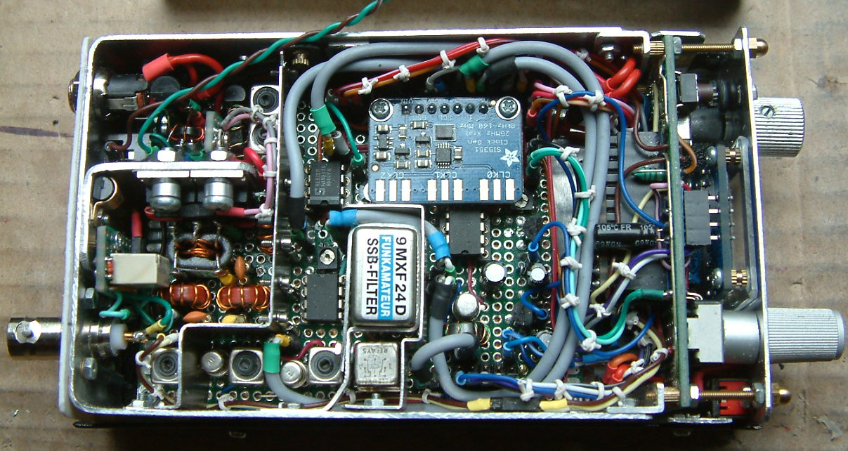
Under the Si5351 breakout the audio amp is hidden. I think available space has been used to the maximum and component density of the board is OK. 😉
Here a view to the underside where all the small SMD components have been placed:
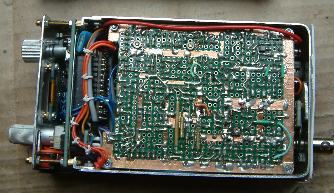
Front panel labeling
Times are getting harder because I’m running short in these adhesive letters that are not available today anymore. An alternative had to be found. Initial tests with the so called “toner transfer method” had been frustrating, but I came across the idea to use labels for laser printers that are cheap and allow individual front panel design.
Here the steps in brief to get a first class front panel labeling:
Step 1: Buy self-adhesive transparency film for laser printers.
Step 2: Scan your front panel using a flat bed scanner:
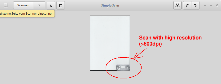
Step 3: Cut the image and work out your front panel. Then enhance the borders of the items you want to label later:
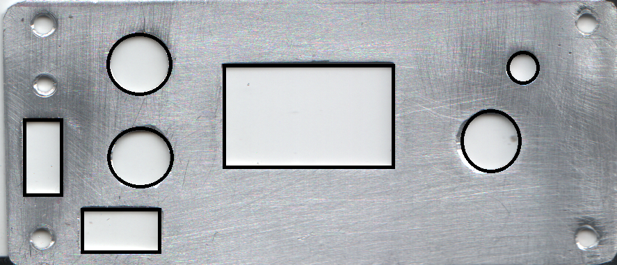
Step 4: Eliminate the background by using the “cut” tool:
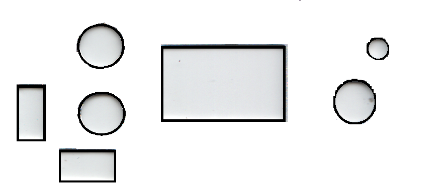
Step 5: Put the labels into the right places and later cut out the borders of the items you have just labelled:
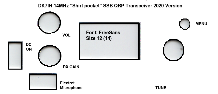
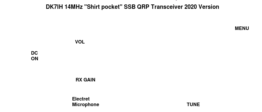
Step 6: Now you are nearly ready to print but one step must be done: Measure the size of your front panel and bring the picture exactly to this size. If you are lucky (like I was) the picture is in the correct dimensions defined by my scanner. If you are not, you can copy the picture to a text processing software or another appropriate tool and adjust the size of picture exactly. Make 4 or 5 five copies on the same sheet and print it out with your laser printer.
Step 7: Clean your front board with grain alcohol and fix one copy of the laser print taking the precise position of the label.
Step 8: Cut the holes and other culverts with a sharp cutter knife or scalpel.
Step 9: Be happy because of having made a top quality front panel!
Mechanical construction
Like its predecessor the radio has been mounted into a U-shaped frame of aluminum. Height is 3 centimeters, thickness of the sheet metal is 1 mm. The front panel has been attached with angle plates also made from Al and fixed with M2 screws. This makes a rugged mounting frame for the veroboard and the additional mechanical structures like sockets for antenna, DC supply and headphone.
To finish the cabinet, a base and a top cover from 0.5 mm aluminum sheets have been bent exactly. Precision is now improved because I started a new method: Before bending the sheet metal I cut a wooden block using a precise buzz saw. In this case case exactly 74 millimeters wide (7 centimeters from the inside, plus 2×1 millimeters for the thickness of the mounting frame and another 2 millimeters of space you need because of the minimum bending radius that is required for the metal sheet. Using this method the cover exactly fits onto the mounting frame.
So, that’s the story of another revision of my radios. Thanks for watching!
73 de Peter (DK7IH)
The Brother PTouch label printer is a good way to make panel labels. You can get Black on Clear tapes, and I think also White on clear as well. Set the printer on a small size font. The labels stick on like scotch tape, and you can spray clear Krylon on top of them for protection. The black on white tapes are good if you have a white panel.
Thankd
בתאריך יום א׳, 28 ביוני 2020, 20:14, מאת Radio Engineering Projects powered by DK7IH (Peter) :
> Peter (DK7IH) posted: “When the project of building a very small > transceiver was accomplished 4 years ago, I still lacked lots of skills in > setting up electronic circuits using SMD technology. The radio’s > craftmanship has been a little bit defective (there were lots of things ” >
Can you post the source code for this? I’d like to see how you mod’ed it from the ad985x to the Si5351.
Hi WA2MZE, the code is also available at my Github site:
https://github.com/DK7IH/Micro26-Rebuilding-my-1st-Shirt-Pocket-Transceiver
vy 73 de Peter
Thanks!
BTW, while the OLED and Si5351 boards you are using may have 3.3 volt regulators AND I2C level converters (so they can be operated on 5v), many of the Chineseium boards don’t. While you must operate these parts from a 3.3 volt power supply (and some boards DO have the 3.3 volt regulators but NOT level converters), you CAN operate the AVR processor on 5 volts with a 3.3 volt I2C bus. The trick here is that I2C is an OPEN COLLECTOR (open drain?) bus with pull up resistors. Just make sure that NO I2C pull ups go to 5v, but rather to 3.3 volts, and make sure that the I2C port lines do NOT have the internal pull ups activated! (The Arduino wire/i2c code would have to have the init code setting the pull ups on commented out!). I didn’t check your code yet, nor do I see any I2C pull up resistors in your schematic. I know the Adafruit board has 3.3 volt pull ups on it, but you might have pull ups to 5v on the arduino nano board (if so remove those two resistors), the OLED board might have pull ups as well. ONLY ONE board needs to have pull up resistors, having more of them (effectively in parallel) might not hurt, but then again? (depends on the length of the bus wiring). In your case, the Adafruit Si5351 is OK for full 5v as it has the level converter, but I don’t know about the specific OLED board you used.
Hi WA2MZE, about the pull-ups for the I²C-bus: I usually use the internal pull-ups in the AVR controller which is sufficient and has never produced any problems.
And for the idea with the 3.3V technology: I have found that the Chinese OLED displays usually work also on 3.3 V. When I use the more modern AVRs that can also run on 3.3V they work well together also with the internal pull-up Rs. Generally spoken, the AVRs and the Chinese OLEDs are very compatible concerning supply voltage.
vy 73 de Peter (DK7IH)
After looking over the code and the SD1306 documentation, I think I see an error in the OLED code. Your oled_command routine calls twi_write to send the I2C address, the control byte (setting C/D to command), and then one command byte, followed by setting the stop condition.
However some commands take two bytes, you seem to send these by calling oled_command twice, but this will terminate the sequence with a stop condition, and then send the address, control byte, and the next command byte. I think the controller is expecting you to call twi_write for each byte of the command, THEN set up a stop condition. You do this correctly to write multiple data bytes in a row. I’d think oled_init would NOT function as desired the way it is written.
The Adafruit ssd1306 library command list loop does this correctly: (command list is passed in as a program memory address pointer)
void Adafruit_SSD1306::ssd1306_commandList(const uint8_t *c, uint8_t n) {
if (wire) { // I2C
wire->beginTransmission(i2caddr);
WIRE_WRITE((uint8_t)0x00); // Co = 0, D/C = 0
uint8_t bytesOut = 1;
while (n–) {
if (bytesOut >= WIRE_MAX) {
wire->endTransmission();
wire->beginTransmission(i2caddr);
WIRE_WRITE((uint8_t)0x00); // Co = 0, D/C = 0
bytesOut = 1;
}
WIRE_WRITE(pgm_read_byte(c++));
bytesOut++;
}
wire->endTransmission();
} else { // SPI — transaction started in calling function
SSD1306_MODE_COMMAND
while (n–)
SPIwrite(pgm_read_byte(c++));
}
}
Hi WA2MZE, I don’t think that my code is faulty because it works perfectly. The routines are extremely fast now (I have revised the code some months ago so that it works also for the “SH1106” OLEDs that are slightly larger than the 1306), no “building-up” of the screen can be observed anymore and I have never encountered any problems. The routines just do what they have to do. 😉
73 de Peter (DK7IH)
It’s possible that the SDD1306 remembers that the last command wasn’t ‘finished’ and correctly picks up where it left off. Still, it might be faster to send all of the command bytes for a multi-byte command in a single I2C transaction, like is down for multiple data bytes. This would involve writing a multi-byte version of oled_command() that takes a string pointer and a length instead of a single byte as an argument. Also since the twi_write() command is used to send the i2c address, you have to set the write bit in the address, which is actually the MSB of the i2c address field. If you were to have a twi_read() function (while your i2c devices are currently used read_only, if you were to add an i2C port extender device, you’d need to be able to read from them), then the I2c address would have to be ANDed with 0x7F to put the TWI in read mode.
I’m planning on experimenting with your code, so I can adapt it for my needs. One thing I’ve discovered is that you can’t run the I2C connection at 400khz, or even 100khz, if the CPU clock speed is only 8mhz. You can reach ~275khz with a 10mhz clock. That’s a non-standard speed, but the slave chips will follow the master clock. (I have an atmega644v I wanted to use. At 10mhz (fasted clock speed) I’d be limited at the twi clock rate. (To reach 400khz the cpu clock must be at least 14.4mhz).
I have an OLED based on the SDD1306 but only 128×32 resolution. I’ll have to rearrange the data on the display to have it fit.
Hi Peter
Just re-read your second iteration of Shirtpocket 20. It is timely as I have recently dome a slight refresh of one of my homebrew projects from a few years back, ‘SummitProwler 5’, my first attempt at a walkie talkie format rig, 40 and 30m, 5 w SSB and CW with pushbuttons on the side to key CW. It needed a few minor improvements (replacement 8×2 LCD, bandpass filter optimisation, substitution of an RF transistor in the Tx driver, replaced a mis-fitting DC jack, re-flashed the MCU, calibration etc. and a little bit of effort has significantly increased my enjoyment of using this rig. Blog post sometime soon.
A few things stood out to me from your account. I’ve used Decadry for decades for labeling, white on black and black on light grey panels, with great results, but boy oh boy, it’s almost im-possible to source now. I don’t know why there is absolutely no worldwide demand for rub on transfer lettering but that is apparently the case. I am getting desperately low. I may have only one more ‘VK3HN” alpha/numeric sequence left! I have not entertained an alternative as per your method as I am clinging onto my long held tradition of run-ons and clear satin enamel spray. Old traditions die hard.
I am interested that a single D.G. MOSFET could match the gain of the MC1350, which I though would have higher gain, obviously not.
Also your TR FET switch is a winner, I saw WA2MZE extended it with 2N7000s which allows it to be driven by a low-going Arduino digital output. Well worth trying.
I see you have replaced your simpler first audio preamp with another design with bypassed emitter, I may try this too, I’ve built your preamp with the grounded emitter ahead of a TDA2003 and found it to work well.
I hope the re-working of this tiny rig enhances your enjoyment of using it, 73 Paul VK3HN.
PS: I’ve ordered a 9MXF24D filter and have already custom designed space on a circuit board for it, will be watching my letter box daily fairly soon.
Hi Paul, thank you very much for your contribution.
1st topic: I think the reason why these rub-on tranfer lettering products are not more available is that applying them is too costly and only for prototyping, if at all. And, as I found out, it is not easy to place the letters exactly so that a 100% precise type face is produced.
2nd: WA2MZE ‘s switch unit looks great but as I don’t need to drive it with an MCU pin I have re-used my older version because of limitted space.
3rd: I have found the MNC1350 has a very steep AGC-voltage -> AGC-gain function which makes producing a well working AGC unit a little more more complicated.
One dual-gate MOSFET does not have the gain of the MC1350 but is very much sufficient. The receiver is very sensitiv. I’m just concerned with developing a switched step attenuator controlled by an MCU to make sensitivity measurements.
But so far I can say that the rx is so sensitive that I can receive signals with “a wet finger”. 😉
The rig has been very much improved and, above all, looks more accurate than its predecessor. That alone was worth the effort. 😉
Vy 73 de Peter
Hi Peter, congrats for a beautiful work and sharing all ideas and circuits. That is what I am calling hamspirit.
Yes, I agree, it is beter to spray front panels. I can confirm that 10 years front panels still lookin good. The front panels I am doing other way – prepare all in Corel Draw, print first on the paper. The paper is used for drilling and cutting. After that I print the film, put it on the front and with a knife do the holes.
Hello Villam, thanks a lot for the idea with the two-step front panel development. Will give that idea a try next time!
vy 73 de Peter
Hallo Peter
What did you use to programmer the Atmega:?
Kleibe
Hi! I use the GNU C-Compiler w. Linux and the AVR-Dude software for uploading. 73 de Peter
Peter, one other idea. The 74HC4053 triple spdt analog switch can replace the dpdt relays used in the filter/NE602 circuit. It would be a good idea to operate the ’53 at +/- 5v and/or AC couple it to the circuits, though many have used it on a single rail 5v supply, operating the ‘602 at 5v. A pair of 74HC4051’s can switch up to 8 BPF’s in/out of the receiver front end (but probably can’t handle the LPF’s at the 5w level!).
(I hate relays!)
Good idea, I remember having these ICs anywhere around here. But before installing them into a transceiver I think some scientific checks have to be made concerning distortion, signal separation, SWR an so on.
vy 73 de Peter
While I haven’t used the 4053 I have used a high quality RF switch, the SA630, an 8 pin SOIC SPDT switch. I got these on special so cost was not an inhibitor. They work perfectly well at HF.
However, compared to a small s.m. relay, the SA630 requires various bypassing, coupling, a 5v supply and all up, adds to the circuit complexity. I prefer to lay out modules in a straight line direction of the signal flow. That usually means a switch at each end. The 4053 and other quad IC switches make this layout difficult as all switches are centralised in a single package. It is very easy to drop a relay onto a board area with a filter or gain stage. I know, they draw 15mA when closed, require a FET to switch the coil from an MCU digital output, and they are mechanical, not electronic. But they are guaranteed to make a reliable connection and can be used to switch RF or DC power.
I will probably unleash further commebts against relays as a result of this comment, but all to the good, a bit of debate is healthy ! Its a matter of personal taste. 73 from Paul VK3HN.
Hi Peter, I am challenged by your build skills they are phenominal. A quick question, do you manually lay out your veroboard, or do you use some software to help you in this process. Your Schematics are well done as well, what are you using? Wonderful builds.
73 Guy N1GMM
Hi Guy, actually I don’t use any software for the layout process with veroboards. It is more or less experience an intution. 😉
For the schematics I have designed a graphics file with all the single elements inside. I use “Copy & Paste” to set up the schematic with the single elements. Basic data is here:
https://radiotransmitter.files.wordpress.com/2020/07/dk7ih_schematic_elements-1.png
Vyx 73 de Peter (DK7IH)
Wow what a super interesting site that is real DIY
Thanks for publishing
That’s how I build my stuff in particular how I make the holes in the front
https://www.youtube.com/watch?v=AqRbZat0tYA&t=378s
My handheld transceiver
https://www.youtube.com/watch?v=QqyVs-ci3QA&t=134s
Looks great! I saw the handheld years before and that gave me inspiration to build my own handheld trx. Congrats! 73 de Peter (DK7IH)