by Peter Baier (DK7IH)
Abstract
We intended to explore, if it is possible to directly frequency modulate a Direct Digital Synthesizer (DDS) with a given sine wave by using a fast microntroller (MCU) and optimized data transfer. The goal was to achieve this by using widely available radio amateur hardware, i. e. low cost equipment.
Frequency modulation (FM)
When applying frequency modulation (FM) a given carrier frequency (f0, marked as (ii)) is deflected from its center frequency by adding or subtracting a certain amount of differential frequency (delta.f) depending on the modulated audio signal (af, marked as (i)). FM therefore is one type of a set of angle modulations, like phase modulation (PM) for example. The variation in frequency by time depends on frequency and volume of the modulated signal.
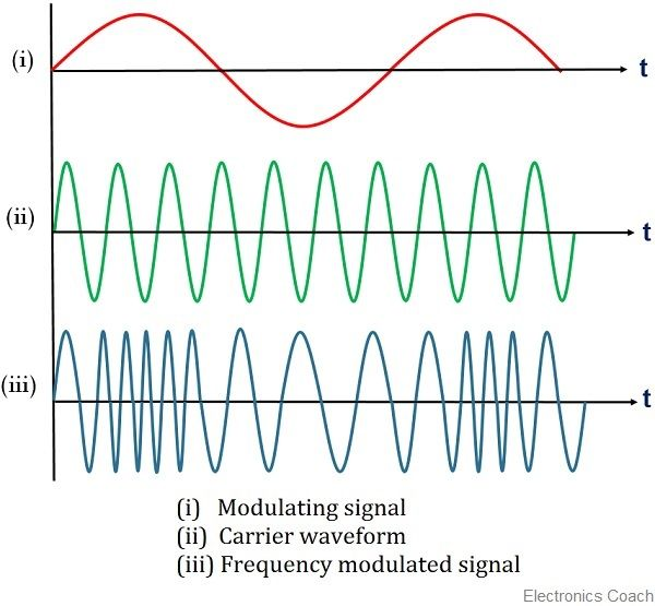
(adapted from https://electronicscoach.com/frequency-modulation.html)
In a “classical” approach FM is produced by feeding the audio signal into an oscillator using a controlling element that is frequency depending. Popular examples for this type of application are varicap diodes (varactors). Thus a “VCO” (voltage controlled oscillator) is the classical and widely used method of an FM generator in radios. For this experiment we want to use a DDS oscillator instead.
Setup
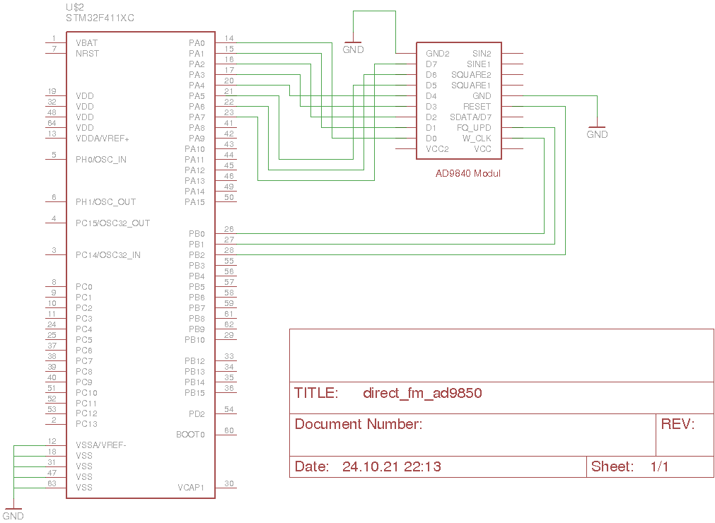
As microntroller unit in this experiment we use an STM32F411 MCU clocked to its maximum speed of 168MHz. As DDS an AD9850 by Analog Devices has been applied. The AD9850 not only offers a serial interface (SPI) which is quite common with these devices but also provides a parallel 8-bit mode data transfer. This enhances data exchange rates by factor of 8 compared to serial SPI mode which should make direct modulation possible.
As MCU hardware a so called “Black Pill” board has been purchased carrying the STM32F411. The AD9850 comes from one of the Chinese made ready-to-use boards. These boards already have all the necessary components integrated, including a 125MHz crystal oscillator. Thus all hardware runs on maximum speed.
Interconnections
MCU and DDS are connected using 8 data and 3 control lines:
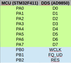
The DDS chip AD9850 is powered to 5V but can be controlled via the 3.3V port pins of the MCU without any problems.
Software
As STMF411 (ARM Cortex(R) M4) MCUs are not “fused” like AVRs e. g. This means that user coded software after having run start-up routines needs to set the internal hardware to the desired clock speed. The “Black Pill” board clocks the MCU with a 25 MHz crystal which is referred to as “HSE” (high speed external). The code lines set various PLLs within the MCU to the appropriate division factors thus generating the desired clock frequencies for the single MCU sections. This is a fairly complex process, thus reading of datasheet and reference manual is recommended for better understanding.
//////////////////////////////////////////////
// Set SystemClock to 168 MHz with 25 MHz HSE
//////////////////////////////////////////////
FLASH->ACR |= 0b010; //2 wait state for 100 MHz
RCC->CR |= (1 << 16); //Activate external clock (HSE: 8 MHz)
while ((RCC->CR & (1 << 17)) == 0); //Wait until HSE is ready

//Configuration of PLL
RCC->PLLCFGR |= (1 << 22); //PLL source is HSE

//Set PLLM
RCC->PLLCFGR &= ~0x3F; //1st Reset bits
RCC->PLLCFGR |= 20; //2nd define VCO input frequency = PLL input clock frequency (f.HSE) / PLLM with 2 ≤ PLLM ≤ 63
//-> f.VCO.in = 25MHz / 8 = 1.25MHz

//Set PLLN: PPLLN defines VCO out frequency
RCC->PLLCFGR &= ~0x7FC0; //1st Reset bits 14:6
RCC->PLLCFGR |= (160 << 6); //2nd define f.VCO.out = f.VCO.in * 160 = 200MHz

//Set PLLP: Main PLL (PLL) division factor for main system clock; Reset Bits 17:16
RCC->PLLCFGR &= ~(0b11 << 16); //Reset bits 17:16
//f.PLL.output.clock = f.VCO.out / 2 = 100MHz

//Set PLLQ. PLLQ = division factor for USB OTG FS, SDIO and random number generator clocks
RCC->PLLCFGR &= ~(0b1111 << 24); //Reset bits 27:24
RCC->PLLCFGR |= (8 << 24); //PLL-Q: f.VCO.out / 8 = 25MHz

RCC->CR |= (1 << 24); //Activate PLL, Bit 24
while ((RCC->CR & (1 << 25)) == 0); //Wait until PLL is ready Bit 25

//Division of clock signal for bus system
RCC->CFGR |= (0b1001 << 4) //AHB divider: 100MHz / 4 = 25 MHz
| (0b100 << 10) //APB1 divider: /2
| (0b100 << 13); //APB2 divider: /2

RCC->CFGR |= 0b10; //Switching to PLL clock source
After this we are nearly already done, but DDS ports have to be configured before as output sources:
//////////////////////////////////////////
// Setup DDS
//////////////////////////////////////////
//Turn on the GPIOA peripheral for DDS
RCC->AHB1ENR |= (1 << 0); //GPIOA enable
RCC->AHB1ENR |= (1 << 1); //GPIOB enable

//Put pin A0..A7 in general purpose output mode (DATA-Port)
for(t1 = 0; t1 < 8; t1 ++)
{
    DDS_DATA_GPIO->MODER |= (1 << (t1 << 1));
    DDS_DATA_GPIO->OSPEEDR |= (3 << (t1 << 1));
}

//Put pin B0..B2 in general purpose output mode (CTRL-Port)
DDS_CTRL_GPIO->MODER |= (1 << (W_CLK << 1));
DDS_CTRL_GPIO->OSPEEDR |= (3 << (W_CLK << 1));
DDS_CTRL_GPIO->MODER |= (1 << (FQ_UD << 1));
DDS_CTRL_GPIO->OSPEEDR |= (3 << (FQ_UD << 1));
DDS_CTRL_GPIO->MODER |= (1 << (RES << 1));

//Reset AD9850
DDS_CTRL_GPIO->ODR |= (1 << RES); //Bit set
delay_us(1000); //wait for > 20ns i. e. 1ms minimum time with _delay_s()
DDS_CTRL_GPIO->ODR &= ~(1 << RES); //Bit erase

set_frequency(f);
set_frequency(f);
Main loop now transfers the numerical values of a sine wave to the output port thus generating the desired frequency shifted by a certain functional value of the sine wave:
while(1)
{
    while(t1 < 360)
    {
        set_frequency(f + sine[t1]);
        t1 += 5;
    }
    t1 = 0;
}
Variable t1 in this case is a shift factor that will use the 360 distinct values of the sine wave array with a certain increment that eventually determines the frequency audible in the receiver.
Full code including functions here not pointed out for this experiment can be found in the full code example on Github.
Results
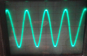
Using a narrow band FM receiver we can read a signal that is is pure sine wave without any noticeable distortion. Audio frequency is about 1 kHz.
Thanks for reading! Peter (DK7IH)