Abstract
On this website we have published various versions of handheld transceivers (Version 1, Version 2) for the shortwave amateur bands. Although they were really useful for successful in-the-field-operation (I do a lot of outdoor sports like cycling and hiking), there were certain shortcomings that had to be overcome with this 3rd version. A lack of output power (Version 1) and the bulky design (Version 2) are the most important things to be mentioned.
So the main design objectives with this third version were:
- Higher RF output (6 to 8 watts PEP at least),
- simple and reliable design,
- low DC power consumption during receive periods,
- more compact size.
The general onset was to reduce receive current draw (as most of the time I use these transceivers on receive mode) and thus being able to insert a smaller battery pack. From the bulky version #2 of the handheld radios I learned that AA cells consume a lot of space thus I intended to switch to AAA cells with approx. 1000mAh capacity.
General ideas on the design
To save DC power in this radio no frequency synthesizer (DDS or PLL) has been used. Instead a varactor (aka “Varicap”) tuned VFO (Colpitts circuit) has been installed as then main frequency generator. This idea also strengthens the experimental approach in amateur radio as it can be considered as challenging to construct an oscillator that is frequency stable without using digital technologies. “Variatio delectat” as the Romans said…
After the usual warm-up phase of about 15 minutes, the frequency is reasonable stable to perform SSB QSOs without the opposite station even noticing the small frequency drift. It figures to around 80 to 100Hz per hour. Also a crystal controlled local oscillator as carrier oscillator and BFO (beat frequency oscillator in the receiver) is present in the design.
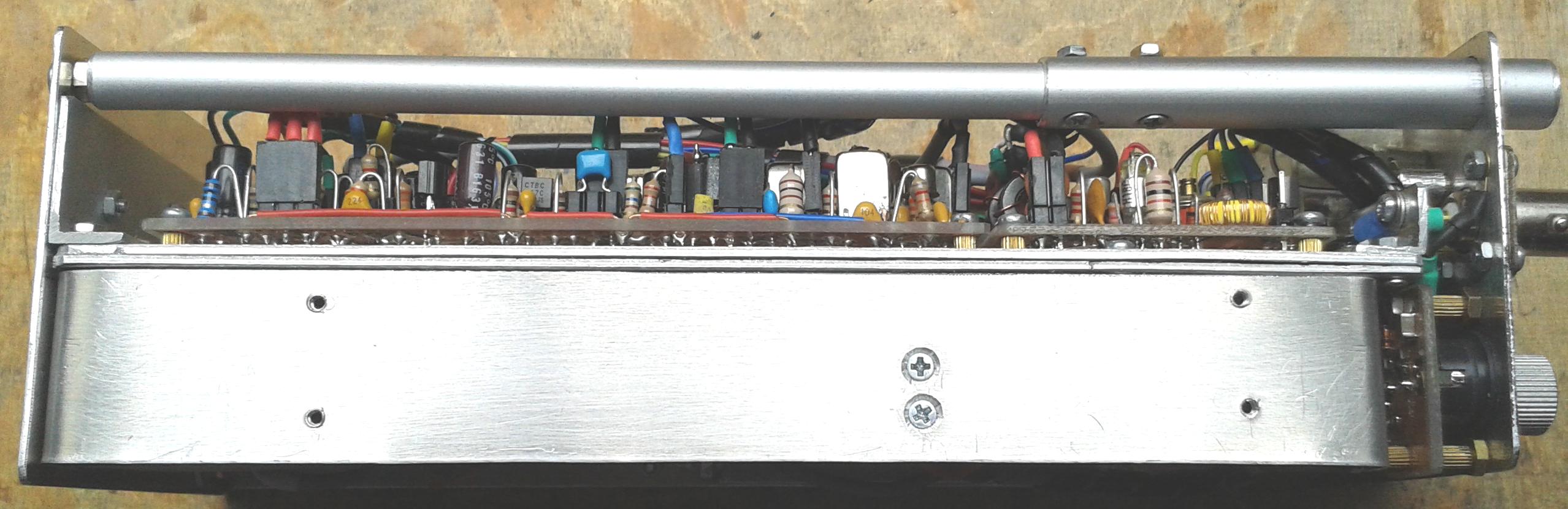
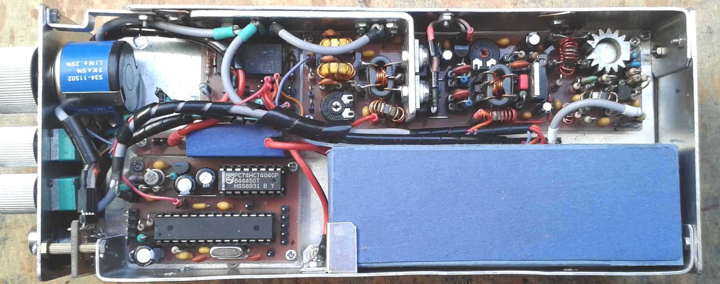
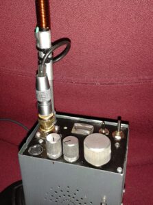
Again a “sandwich” structure has been applied to carry all the electronics inside the radio. With the PCBs that are about 25 to 30 millimeters in height (with components) there was enough space for 2 boards “back to back” not to exceed the height limit of 6 centimeters that I defined still to be “handy”. Thus the whole design could be realized on two aluminum plates (1.5 mm thickness) as carriers for the whole construction. Front and back plates are held in place either by aluminum angles plus screws, bolts and spacers of the 2mm thread material available from Chinese internet vendors.
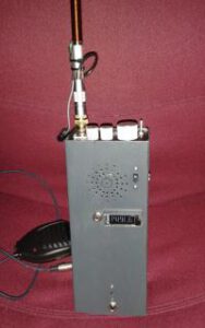
A guide tube for a “plug in” rod antenna also has been installed (please see picture above!)
The whole radio now measures 60 mm in height, 80 mm in width and about 190 mm in length.
1. The Circuit
1.1 Section #1
This compartment consists of the 2 oscillators, the receiver section and the SSB generator plus transmit mixer. The upper and the lower section are connected using a 2.54 millimeter (0.1″) header strip to feed through various lines between the two sections.
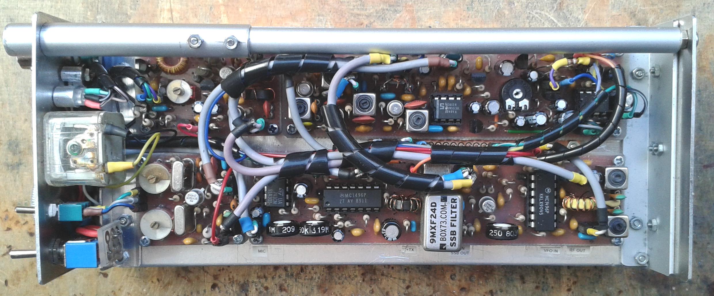
On the left there are the two oscillators (VFO in top position, LO at the bottom), The SSB generator (bottom) and the receiver unit in top position of the picture are on the right side. The SSB filter is connected using shielded cables to the receiver section.
The schematics for the various PCBs plus the respective layout for each single PCB:
1.1.1 The VFO
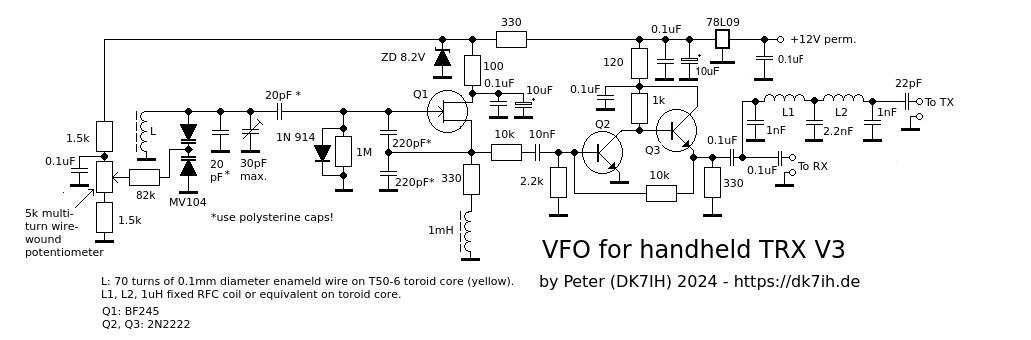
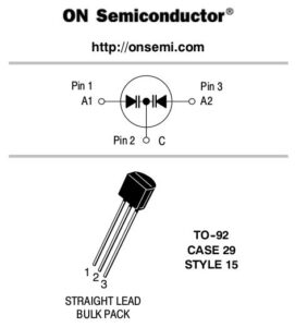
Main tuning element in this VFO is an MV104 tuning diode that is used in FM receivers for electronic tuning. Inside the TO-92 housing there are 2 varicaps with cathodes connected. This is the point to apply the tuning voltage. The anodes are connected to GND either directly or via the coil in the tuning circuit. To decouple the tuning circuit from the control DC an 82kΩ resistor is appropriate.
The diode has a voltage=>capacitance ratio that makes it interesting for this VFO:
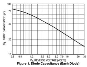
In the voltage range between 1 and 7V that we are about to use the slope is relatively linear. Capacitance in this range falls into an interval from 60 (U=1V) down to 28 pF (U=7V). As the value refers to one single diode and the total capacitance halves because of the two diodes in series we can expect a range in capacitance from about 14 to 30 pF.
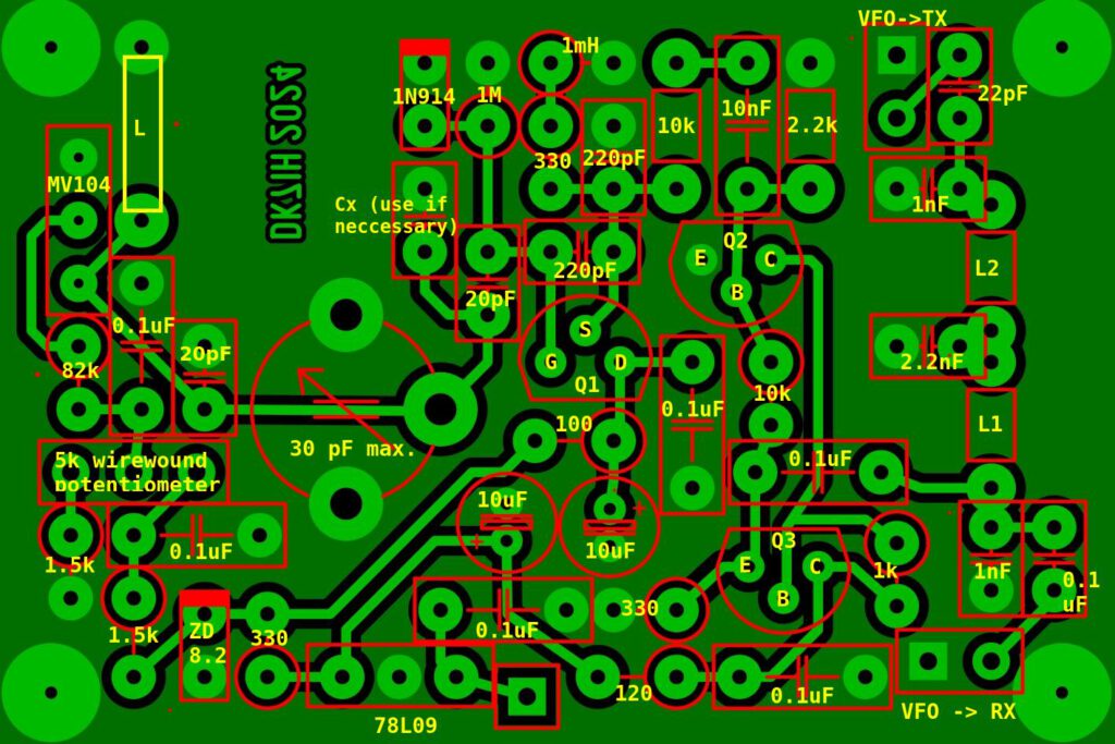
As the interfrequency of the radio is 9MHz the VFO is tuned in the 5…5.35MHz range. The coil’s inductance (70 turns on a T37-6 toroid core (yellow)) is about 14.7uH. To come to the lower end of the frequency range a parallel C of total 68pF (approx.) is required. This is composed by the varactor, the parallel fixed value C (C=20pF), the plastic trimmer and (in series via the 20pF coupler) the two 120pF capacitors that are used for the 180° phase shift network in the transistor to make the device oscillate. As all the components are highly crucial for frequency stability they should all be made of polysterine. Ceramic capacitors are a true “NO-GO” in this place. Some designers recommend NP0 ceramics which can be useful in some cases. But as this VFO is designed for optimized balancing the temperature coefficients of the tuning coil (70 turns on a T37-6 toroid), the 30pF plastic trimmer and the MV104 tuning cap we did not experience the need for NP0 ceramic capacitors.
For feeding the DC tuning voltage into the varactor a multi-turn wired potentiometer with 5k total resistance has been built in. There are two resistors (1.5k each) in series with the pot. This is to limit the voltage span reaching from 1 to 7V as mentioned before. So we can use the full swing of the 10 turns in the pot to map the oscillator into the range of 350kHz frequency width without losing too much tuning space leading to out-of-band frequency. The tuning voltage is stabilized twice: First by an 78L09 voltage regulator feeding the whole VFO and later with an 8.2V Zener diode. If possible, the 78L09 should be replaced by a low-drop version.
The tuning stage is followed by a two staged buffer amplifier (stages directly coupled) to decouple the 1st stage as strong as possible from the output. The coupling between the oscillator stage and the buffer is very loose due to a 10kΩ resistor in series with the first stage’s RF output.
There are two outputs within the VFO:
- an unfiltered one for the receiver and
- a low pass filtered one for the transmitter.
A low pass filter (LPF) in the transmitter’s RF line has been used to minimize the voltage of the oscillator’s 3rd harmonic (around 15 MHz) feed through that falls into the range of the 14MHz band pass filters succeeding the transmit mixer.
The VFO’s output voltage (unfiltered) is about 3Vpp.
The PCB is designed as follows. Hint: On the PCB there has been an additional location for another parallel C (not in the schematic) if the user should need to insert another cap.
1.1.2 Local Oscillator
This oscillator also uses a Colpitts circuit.
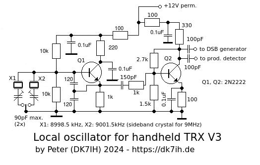
There are two different crystals, one for each sideband:
- 8998.5 kHz (USB)
- 9001.5 kHz (LSB)
Frequency calculation scheme with 2 audio signals applied to the modulator:
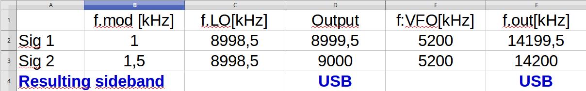
The optimized carrier frequency is adjusted by tuning the variable capacity in series to the respective crystal for best pitch sound in the receiver as well as suitable frequency response curve in the transmitter (using a tunable audio signal oscillator for example). Listening to the completed radio in one of the internet SDRs can also be helpful in judging the correct audio frequency response curve.
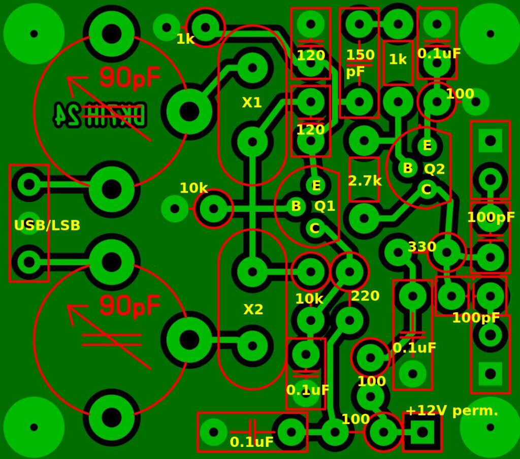
The PCB layout:
1.1.3. The Receiver
The receiver uses one of my “proved-to-be-working” designs that I have applied in other radios with good success:
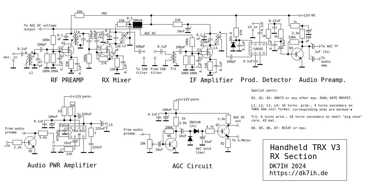
The first 3 stages are equipped with dual gate MOSFETs like the nowadays obsolete 40673. But every other equivalent can be used here, including SMD parts (BF998 for example) on a breakout board.
The 1st stage is an RF amplifier with a tuned circuit each in the input and the output. Mind the orientation of the tuned and untuned parts of the LC circuits. On the one hand the high Z end of LC1 is fed into gate 1 of the dual gate MOSFET due to its high impedance. On the other hand the goal is to avoid two tuned circuits on the input AND the output of the stage which would make the stage very prone to self-oscillation. So the input is tuned, the output is not.
This stage provides excellent selectivity concerning strong signal out of the band. Particularly during the current high sun activity the 22m broadcast band is prone to interfere with the weaker signals on the 20m amateur band. The second stage also uses a dual gate MOSFET and works as a the receiver’s mixer. Dual gate MOSFETs used as mixer have reasonable dynamic range and are not sensitive to high signal amplitudes and resulting cross modulation. The input voltage coming from the LO on the other hand must be fairly high. 2 to 3Vpp. are the recommended minimum value.
LC3 is tuned to the interfrequency. As all inductors have the same windings (16 turns primary, 4 turns secondary on small TOKO coil former) the parallel capacitor here is 100 to 120 pF instead the 47pF used in the 14MHz stages.
After the filter the incoming SSB signal is fed into a transformer (Tr1) with a 1:9 impedance ratio to match the high Z of the dual gate MOSFET’s (Q3) gate #1 impedance.
The interfrequency amplifier uses nearly the same circuit as the input amplifier. Both gate #2 connectors are supplied by the AGC voltage using a 2:1 voltage divider. Thus the resulting control voltage ranges from approximately 0V to 6.5V (1/2 VDD). Gain of these stages is a proportional function of the AGC voltage, so low voltage means low gain.
The product detector uses a SA602 mixer circuit providing about 12 to 16dB gain as well.
An audio low pass filter (2 resistors with 1k each and two capacitors) completes this stage to make the receiver sound more pleasant by eliminating high frequency hiss sounds in the audio signal.
Audio preamp and power stage are equipped with a single bipolar transistor and the TBA820M IC which works more stable than the “usual suspect” in this stage, the LM386.
The AGC (automatic gain control) uses the audio voltage to derive the DC voltage fed into the AGC chain. A 33uF time constant capacitor is appropriate with the signal characteristics of an SSB signal concerning hold time.
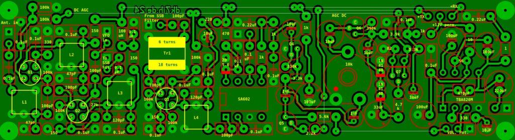
The PCB for this receiver board:
1.1.4 SSB Generator and Transmit Mixer
This construction has been designed to avoid extensive usage of the NE612 IC (or its equivalents). So I used the more enhanced MC1496N Gilbert cell mixer by Motorola (nowadays available from ON semiconductors). This is due to the fact that carrier suppression (to my experience) is better in the MC1496 than the NE602. This pays even if the circuit is more complicated.
The full schematic:
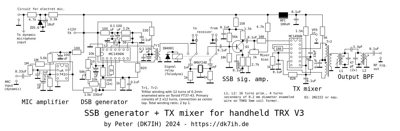
The radio can be equipped with a microphone either the dynamic type or the electret version. For the latter purpose an adapter board for the “Mini DIN” microphone jack has been designed. This will be shown later in this text. The board provides a approx. 2V DC supply on the audio line for an electret microphone.
The microphone amp uses an operational amplifier with adjustable audio voltage to set the appropriate level of microphone gain.
The MC1496N is used according to the data sheet application with single rail power supply. The output is symmetrical which uses all two outputs to enhance gain slightly (pins 6 and 12) in the range of 3 to 4 dB. Next the 9MHz SSB filter follows. After that we see an A-mode signal amp to enhance the signal level in the range of about 15dB. The TX mixer is the last stage in this module. Here the mixer bias also is adjustable to make sure that gain set is appropriate particularly concerning linearity and waveform. In case the transmitter should not be sufficient concerning IMD3 value this trimmer should be tried to improve performance. A two-stage band filter completes the SSB-14MHz-generator.
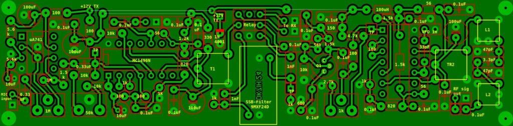
The PCB:
1.2 Section #2
On this layer we find the radio frequency power transmitter, the DC switch board, frequency counter and the battery pack (1000mAh).
1.2.1 The RF power transmitter
This is a design using four stages. The design is based on the predecessors of the radio where 3 stages have been used did not have enough output power. This circuit is able to provide 10+ watts on the 14MHz band but has been limited to about 8 watts PEP due to save battery power and to improve IMD3 performance.
The schematic:
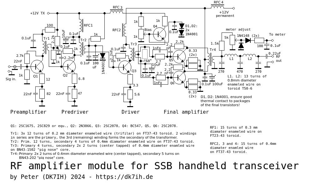
All stages are equipped with bipolar transistors because of an author’s allergy towards RF power FETs 😉 .To ensure top performance concerning transmitter linearity various measures of providing negative feedback have been used.
On the one hand there is emitter degeneration in each stage consisting of an unbypassed resistor about 1/4 to 1/10 of the main resistor to GND. Second there is negative feedback between base and collector in each stage. During experiments these values have been optimized to find a suitable compromise between gain and signal quality.
Stages 1 and 2 are in mode A whereas stage 3 and 4 are in mode AB. Appropriate bias in the power stages 3 and 4 is provided either by a single diode and a current limiting resistor with 1k value (stage 3) or an adjustable bias set (stage 4) using a bipolar transistor. This trimmer should be set to a quiescent current of about 60 to 80mA.
It also should be made sure that there is good thermal contact between the diodes and each of the transistors. As the transistor gets warmer the diode increases its conductivity thus there is more current towards ground (GND) which will reduce the base current in the stage. This method ensures good protection against thermal runaway of the respective stage.
The low pass filter finishing this module should also be carefully observed. Controlling the harmonics using a spectrum analyzer is a good idea. Particularly the first harmonic in the range of 28MHz should be checked. It has to be 20 to 30dB below the main signal on 14MHz.
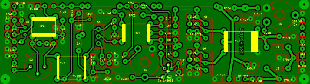
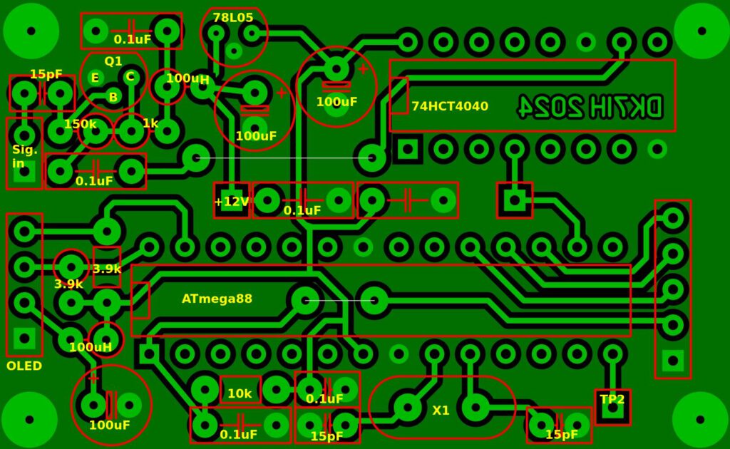
1.2.2 Frequency counter
As there is a VFO for the frequency generator we should integrate a frequency counter to control the operating frequency. This is a very simple unit, DC current is about 10 to 12 mA:
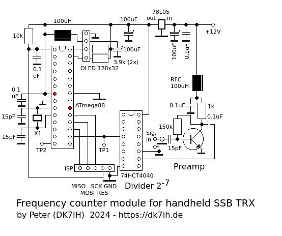
The module is based on an 8-bit microcontroller (MCU=ATmega88) and the respective software. The MCU is clocked with its maximum clock rate (20MHz) which is determined by crystal X1 in the schematic. A binary ripple counter IC (74HCT4040) divides the input frequency by the factor of 128. This signal is fed into the digital input of the microcontroller. A small 128×32 OLED provides the digital readout to the user.
To decouple the VFO output from the 74HCT4040 IC input a preamplifier with a small capacitor (15pF) has been installed here. Q1 can any E-B-C pinout transistor with suitable fT like the 2N2222 for example.
1.2.3 DC switchboard for TX and RX
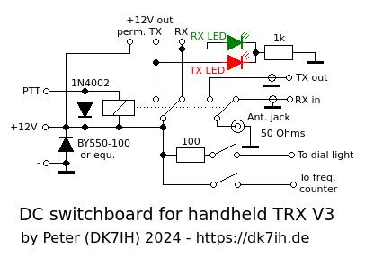
In this radio I haven’t used POWER FETs to do the transmit/receive switching but a 12 Volt relay that was surplus in my junk box.
This board also includes the switchable DC power supply for the meter light (in series with a 150Ω resistor). As the dial light in the meter draws about 25mA from the battery when lit, this gives us large potential to save battery power.
The PTT line is switched to GND. A clamp diode (D1, e. g. the 1N4002) eliminates voltage peeks generated by self inductance in the relay’s coil. And there is also a false polarity protection diode (D2, any high current >=5A silicon diode) integrated that will blow a fuse (visible under the small blue cardboard cover in the picture above) when the battery pack should be connected in the false sense. But as we all know, such things NEVER happen! 😉
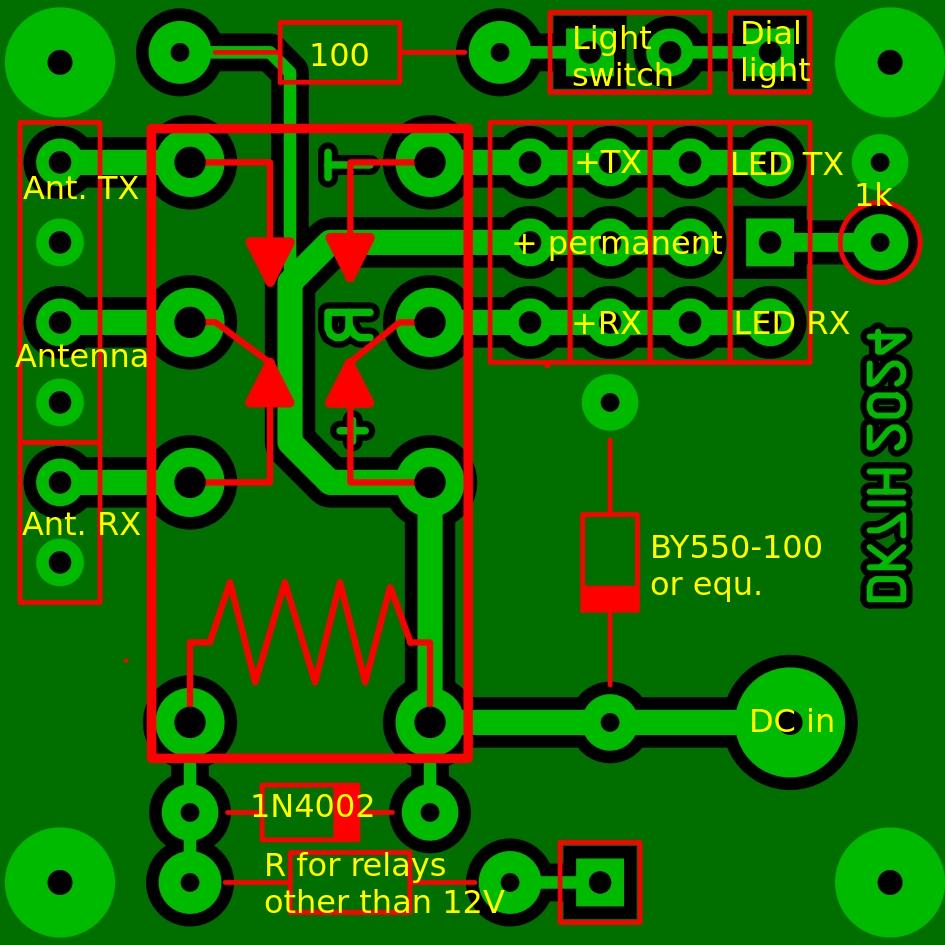
The PCB for this unit:
1.2.4 The battery pack
The battery pack is made of 11 pieces of NiMH cells with 1000mAh capacity each. The connectors are soldered together and have been coated with a box made of cardboard. Also in the interior there are cardboard strips to prevent short circuits in the box. This battery pack is fixed with a clamp made of aluminum that is screwed to the outer boundaries of the enclosure.
Charging should be stopped when the battery voltage reaches 15.9 Volts. The minimum voltage should not fall below 11.5V (approx.).
1.2.5 MISC
A fuseboard has been integrated between the battery and the DC switchboard module:
![]()
The current to charge the battery is supplied from a standard DC jack integrated into the front cover. In series there is a small light bulb. As metals (and thus the thin wire inside the bulb) have positive temperature coefficient (PTC), this simple circuit delivers a more or less constant current to the NiMH battery pack without involving complicated regulator circuitry. A laptop charger with 20V DC (approx.) is OK for refilling the battery but because of the switching noise it is not big fun to listen to the radio during these times. An other alternative could be a solar panel.
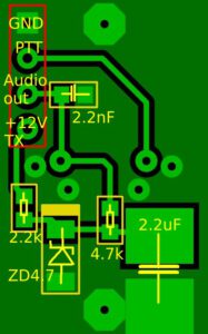
For carrying the “Mini DIN” microphone jack and supplying an appropriate DC voltage to the electret microphone there is a board that is to be inserted into the front panel:
The space in this section is very much limited which made it necessary to use SMD components for this part. The standard “Mini DIN” jack is in the center of the small PCB, the components used for the DC voltage supply surround the microphone jack.
A 4 pin 2,54mm/0.1″ male header strip is used to connect the transceiver circuits to the microphone jack board.
2. Antenna
As this radio is for portable use (like SOTA, POTA etc.) a rod antenna is the favorite antenna even with the problems shortened antennas cause. Here to be mentioned are impedance values of lower than 50Ω as well as lower efficiency.
To mount the antenna a guiding rod and a BNC jack for the shielded cable have been installed into the front panel. So a “plug in” rod antenna can be mounted. But this construction also makes it possible to use a base station aerial. So, it is all in all a very versatile device.
The rod antenna for portable use is made of 4 single elements. 3 of them are from aluminum tubes (available in the local hardware store), that fit neatly into each other. The starting diameter is 8mm, then 6 and the last is 4 mm. The 4th element has in former times been a telescopic antenna taken from a remote control device.
The elements are either connected by screws and bolts or by a threaded rod. The last element is put into its predecessor using a 4mm “banana” plug. The antenna made mainly from aluminum causes a relatively low torque which means that the radio can be handled comfortably by the user during walking or standing.
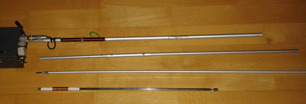
The two coils (one bottom, one more or less “centered”) are wound on PVC rod (bottom coil) or PVC tubing (center coil). The lower coil is made of 0.8 mm enabled wire (50 turns on an 8mm PVC rod) with a moveable hose clamp for optimized length adjustment. A VNA like the “NanoVNA” helps tuning the antenna to a certain degree of precision.
The copper wire has been treated with sandpaper or a file at one side to get rid of the insulating wire and to ensure good contact with the clamp.The clamp usually short circuits one winding but this turned out to be neglectable.
The upper coil consists of 30 turns of 0.6 mm diameter enameled wire.
A GND lead close to the antenna feeding point is connected to a small piece of flexible cable with a banana socket where 5 meters of wire can be connected to increase the antenna’s efficiency forming the 2nd half of a dipole.
3 Results
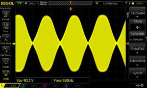
The transmitter’s output power is about 8 to 10 watts PEP with fully charged battery. The modulation and the spectrum in the 14MHz frequency band using a two-tone generator as audio source can be examined with the respective pictures:
As Vpp. in this measurement equals about 63V this means that power (PEP) is exactly 10 Watts.
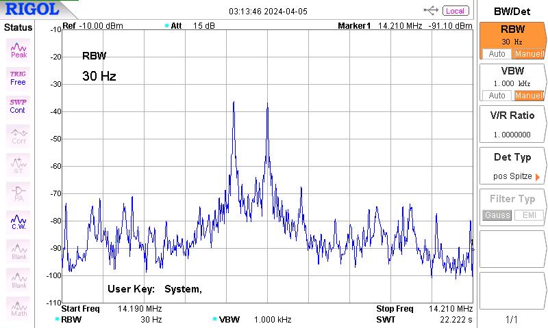
IMD3 is 30 resp. 35 dB below peak voltage.
On receive the battery pack (1000mAh) lasts about 10 hours which is determined by the final discharge voltage which is about 1.1V per cell according to [1]. The receiver consumes about 80mA with dial light switched off. The frequency counter here is in the range of max. 15mA, most of the time between 10 and 12mA. Additional power saving could be achieved by switching off the counter as well.
Receiver sensitivity is extremely high. Receiving signals is possible just by touching the “hot” lead in the antenna jack with a paper clip. On the other hand even very strong stations are no problem to receive without distortion as the AGC circuit delivers high gain compensation in the range of >55dB.
Frequency stability is more than sufficient for an SSB transceiver. Long-term drift analysis reveals drifts of about 80 to 100Hz per hour on receive mode. Longer transmit times have not been examined but with “standard” transmissions using SSB frequency drift seems not to be enhanced compared to receive mode. This might be due to the construction that positioned VFO and PA amplifier in different compartments of the housing. Even if the aluminum frame provides good heat conductivity this seems not to take negative effect when transmitting time shares are moderate.
Thanks for reading!
VY 73 de Peter (DK7IH)