A word to the numerous spammers using this article to spam my website: It’s completely wasted time to copy & paste nonsens messages like “I used to be able to find good advice from your blog posts.” etc. together with an URL to enhance search engine scoring for your website. I read ALL the comments submitted and put them to trash instantly when they have got nothing to do with the technical topic of this (and all other) articles. So my advice: Don’t do it! You’re just wasting time!
by Peter Rachow (DK7IH)
After having built my first shirt-pocket transceiver about a year ago I occasionally thought of how this or a more or less modified design could be made simpler to save components and therefore limit space as well as reducing the complexity of the whole rig. This was due to the fact that I thought that the ancestor (see link above!) of this project was somehow „overkill“ because I used plenty of stages redundantly that could have been used for receive and transmit operation.
Before we go into the details of this new project, let’s have a look on the new micro transceiver (here operating portable as EA8/DK7IH/QRP from the island of Fuerteventura):
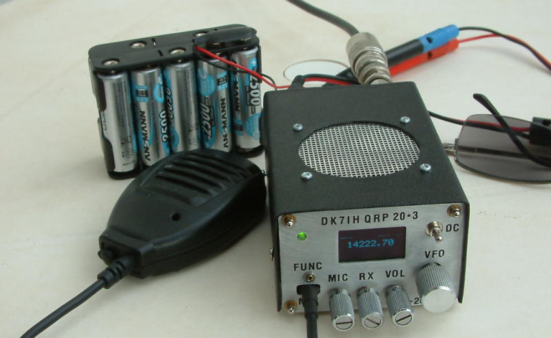
Cabinet size is about 10 by 4 by 5.5 centimeters which equals to a volume of 220 cubic centimeters (cm³).
Making it more simple without detereorating the performance?
Under the aspect of simplifying the circuit I remembered that I had searched for simple designs of transceiver circuits some years ago intensely. After having revisited some of them on the Internet my attention was caught by the „Antek“-Transceiver that has been published by SP5AHT a while ago. This was an ideal basis for my purpose because I intended to build a „2 mixers+1 filter“ circuit in order to make at least 2 of the 4 mixers that are necessary for a fully functionally SSB transceiver redundant. The central part of SP5AHT’s design matched my requirements in an ideal way:
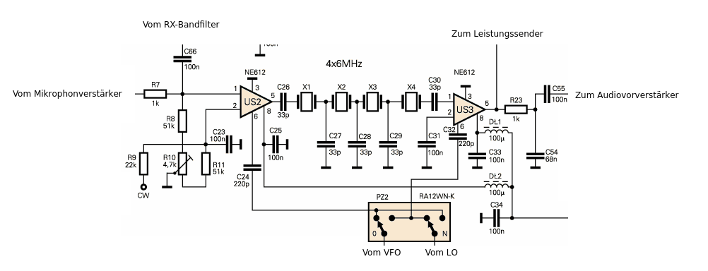
SP5AHT’s circuit uses one mixer (US2 in the schematic) to serve as the receive mixer during rx periods and for the balanced modulator when on transmit. Then the resulting signal is fed through the filter and subsequently processed by mixer 2 (US3). This mixer works as the product detector on receive mode and as transmit mixer when you are on the air. The two oscillators (VFO and LO) are fed to the respective mixer depending on the current operation. This is done by a simple relay connected to the PTT. So when changing from receive to transmit the two oscillators are swapped thus changing the complete function of the circuit.
To get rid of the relay and because I wanted to use the Si5351A clock oscillator chip, my idea was making two of the 3 oscillators present in the clock chip act as LO and VFO. By software, when switching from rx to tx, these oscillators’ frequencies are simply swapped. The microcontroller driving the Si5351A reads the PTT and when pressed to talk the frequencies present on CLK0 and CLK1 are put out reversely. Thus no hardware switching is required.
In addition the audio amps in the end of the receiver chain are powered off. Instead of this the rf power amp of the transmitter section is connected to +12V DC as well as the microphone amp. The antenna relay disconnects the receiver front end from the antenna line and connects the antenna to the LPF that is installed after the rf power transformer of the rf power amp final stage.
By this the whole transceiver is constructed much simpler and lots of circuitry has been removed from the rig.
The block diagram
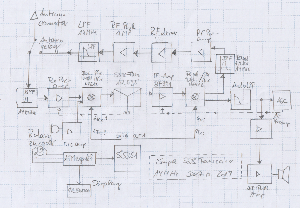
Circuit explanation: During receive periods the signal is fed into the antenna jack whose line is switched by the antenna relay and fed to the first band pass filter for 14MHz when listening to the band. Afterwards it is amplified by a dual-gate MOSFET transistor that is connected to the AGC line that reduces gain when strong signals are detected. The next stage is mixer 1 where a VFO signal of about 24 MHz comes from CLK0 of the Si5351A module.
The result of this mixing process is the IF of about 9 or 10.7 MHz or whatever frequency you are about to use depending on the filter you have installed. This signal is amplified by another dual-gate MOSFET. On receive mode this stage is also under AGC control. When transmitting it is powered to full gain of about 18dB applying +12V via a 2:1 voltage divider consisting of 2 resistors with 82k each.
Next step is mixer 2 where the IF signal is mixed with a 9 resp. 10.7 MHz LO signal (receive mode serving a product detector) or with the VFO signal in mixer 2 serving as tx mixer.
On receive two audio stages (a preamp with LPF in advance and a power amp) amplify the audio signal to a level that can be fed into an 8 Ohm loudspeaker.
On transmit a BPF eliminates the unwanted mixing products and a three stage rf power amplifier lifts the signal to a power level of 3 watts peak power.
The Main RF Section
This central section of the rig consists of the two mixers mentioned before, a off-the-shelf made (in my case) 10.695 MHz filter stripped from an old CB radio, some amplifier stages and so on. The circuit is the following one:
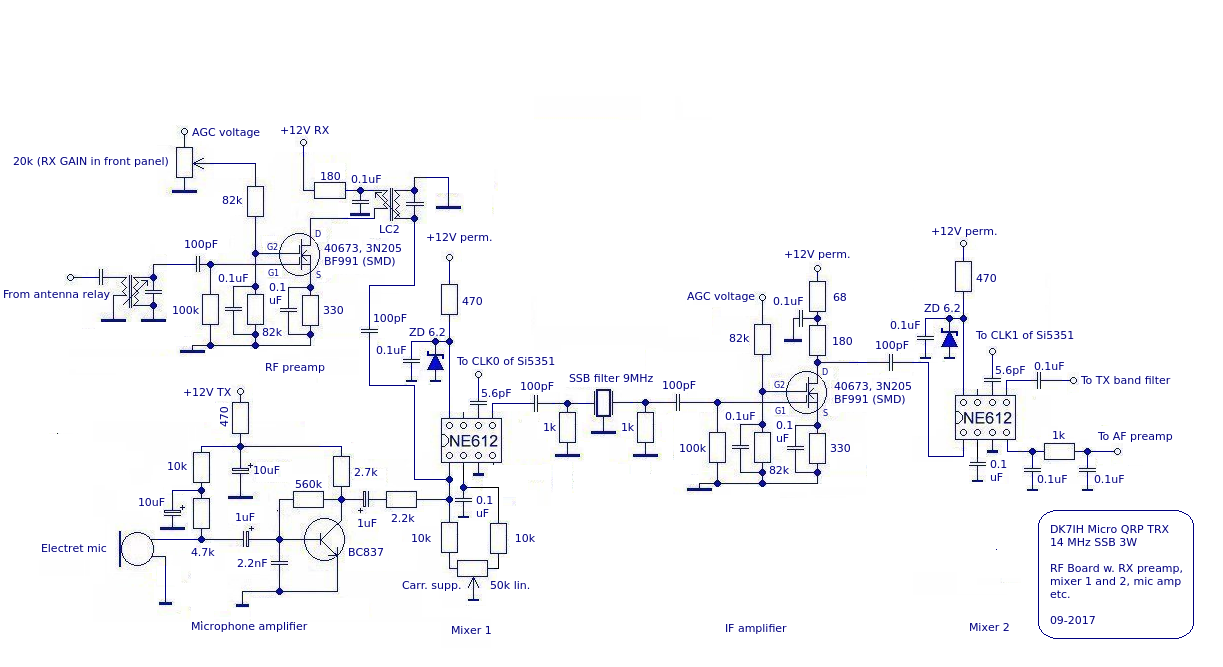
Starting from left side top there is the first receiver amplifier stage using a dual-gate MOSFET. The use of a MOSFET transistor ensures that the noise figure and sensitivity of the whole receive improve very much. The stage is comnnected to the AGC chain. The dc voltage applied by the AGC section varies in the range from 0 to 6 V DC. In addition it can be set by hand by turning a front panel mounted potentiometer that alters the DC voltage in the range from 0 volts to max. volts from the ADC section.
The input is a single tuned circuit using 4 (antenna side) by 16 turns (MOSFET gate side) on a TOKO 5,5 mm coil former. Parallel capacity is 47 pF. In drain line of the transistor the same filter is used coupling the signal to the first mixer (NE612). Note that the second filter is reversed (secondary in drain line) to avoid self-oscillation of the preamp stage.
This mixer’s signal is fed with 2 different input signals (antenna or microphone) and with 2 different oscillator frequencies: about 24 MHz on receive mode or 10.695 +/- 1.5 kHz depending on sideband used when on transmit. The resulting interfrequency signal is fed into an SSB filter which is terminated by 2 resistors of 1k each side to ensure proper impedance matching.
Next stage is the interfrequency amplifier which is the same circuit like the receiver’s preamplifier. This one is also connected to the AGC’s DC line. On transmit mode with no AF signal on the AGC present this stage runs on full gain.
The chain is completed by the second mixer serving as product detector on receive and as tx mixer when going “on the air”.
The audio and AGC section
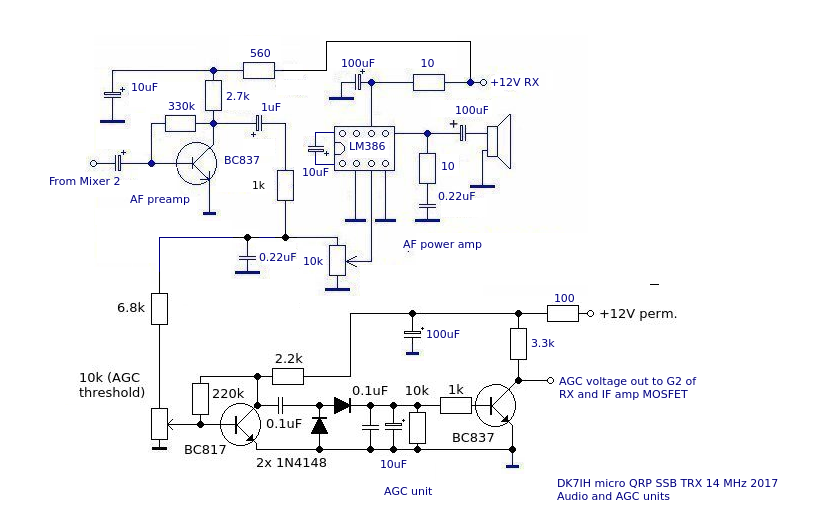
This section also is no “rocket science”. A simple preamplifier using a bipolar transistor (BC846) in common emitter mode, a low pass filter (R=1k and C=0.22uF) and an LM 386 amplify the resulting af sig to an adequate volume to listen to the sound even in an environment that is not 100% noise free.
The RF power module
This is a circuit I have built several times and it’s capable of delivering up to 5 watts of rf power. In this transmitter I’m not driving it beyond 3 watts which is suffice to establish connections on the 20 meter band worldwide a well performing antenna provided.
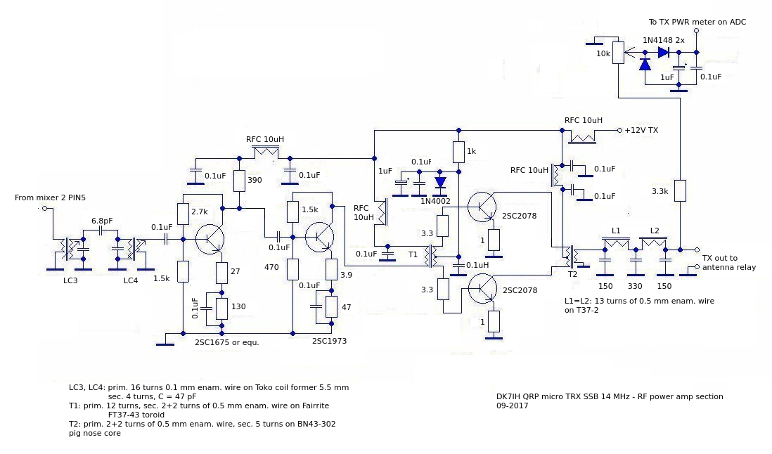
Emitter degeneration and negative feedback are present in preamp and driver stage to ensure maximum linearity. Both stages are operated in class A mode. The final stage works as a push-pull stage using class AB. Push-pull mode eliminates even order harmonics by circuit feature. A heatsink is mandatory for the final stage (the mounting frame in my case) and at least recommended for the driver. The values for the broadband transformers are stated in the schematic above.
The VFO module
This one is equipped with the clock oscillator chip Si5351A by Silicon Labs. I use it mounted to the well known Adafruit breakout board that can handle 5 volts even if the chip is designed for 3.3V. So, this board is compatible to standard microcontrollers like the ATmega168 that is applied in my transceiver. The display is the 1306 chipset based OLED that is also designed for 5 volts supply voltage. Both, the Si5351 and the OLED are designed for I²C-interface which is called “Two Wire Interface” (TWI) in Atmel’s language. The major advantage this interface has got is that only 2 control lines are required, one of them clock (SCL) and the other data line (SDA) to transfer data to the respective units. Basically you need two pull up resistors to tie these lines to +5VDD but I use the internal pull-up resistors in the Atmega168’s ports that do the job well.
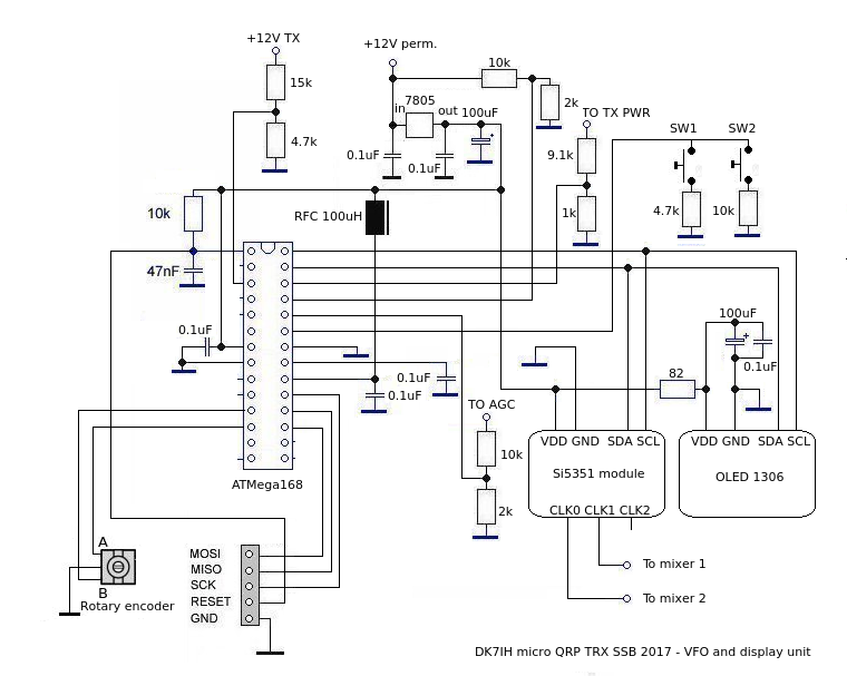
Problem to be mentioned: When testing the early version of the receiver I found the OLED to be very noisy. After a brief research I realized that the signals that were audible in the receiver traveled on the VDD line. Thus I inserted an 82R series resistor and a set of blocking capacitors in the place which made the noise fully disappear.
Practical setup
The main board of the transceiver is made of a 5 by 7 cm breadboard with double-sided soldering pads each connected by a small tubing electrically connecting the both sides of the pad . This is a big advantage when you solder SMD components because you can setup the circuit on both sides of the board and save a lot of space. NExt is that it is nearly impossible to dissolder the pads even if you are resoldering the spots many times. The reason: The soldering pads are rivets anchored on both sides of the carrier of the board.
The components that aren’t available in SMT are standard through-hole but there are only a few like the SSB filter or some old 40673s I used instead of e. g. BF991. Coils for low power are wound on TOKO 5.5 mm coil formers. Power rf transformers are connected to soldering nails in the board. The inside view plus a centimeter scale:
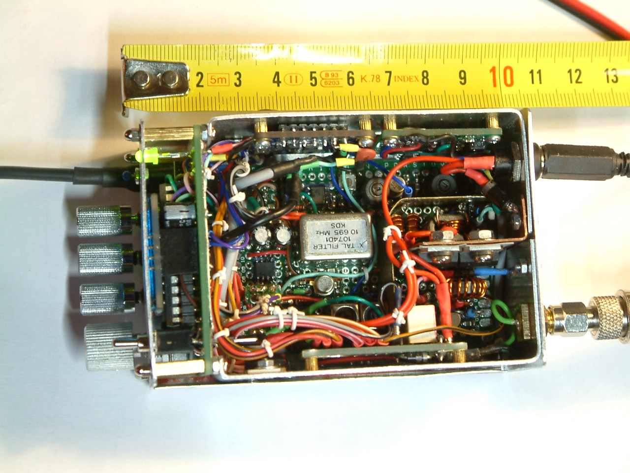
On the left you can see the front panel with the controls, behind the panel the OLED and then the main rf board. The Si5351 is mounted vertically on top left from the AGC board. Underneath there is the receiver’s front end (hidden by the red power supply cable). On the right I sited the power transmitter, at the bottom there is the relay for tx/rx switching. All is built into a 9 * 5.5 * 4 cm Aluminum frame.
Being “on air” with the rig
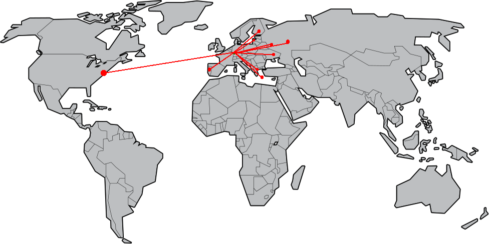
Operating is really fun with this micro transceiver. Since the finishing of the transceiver 4 weeks ago I was on air daily. Here are some regions of the world I could establish successful contacts with. Antenna is a Delta Loop fed in on upper corner about 12 meters above ground.
Plans for the future
Several options may be my next project: First I got plans are to expand this rig to a multibander (due to Si5351’s capabilites of generating max. 160MHz signals), build a PA of about 30 watts max. power (with 2 transistors 2SC1969 in push-pull mode) or to rebuild the transceiver for 17 meter band and hoping that conditions will be better the next couple of years. Let’s see what the real deal will be! 😉
73 de Peter (DK7IH)
Hi Peter
Congratulation on your new design, I think it is a brilliant concept and I am looking forward to further
developments
73
John ZL2TCA
Thank you John, I’ll keep on trying my very best! 😉
Hi Peter. How about the atmega code? This could be used to another bands?
73 kleibe PP2KR
Hi PP2KR, no problem. As soon as I will have returned home from vacation, I will post it here. 73 de Peter
Hallo Peter,
is there a reason why you don’t use both ends of the LC2 transformer to supply the NE612 with a balanced input signal? I think this would improve performance by a lot.
Viele Grüße
Hi Felix,
I have tried a symmetrical coupling in a former transceiver and compared it to the unbalanced. I could not find a significant difference in performance if either. And in this special case putting the “cold” end to PIN2 of NE602 would interfere with the balancer circuit of the SSB modulator if not coupled with a C e. g. 100pF. To keep the circuit simple I did not try this.
73 de Peter
Peter. Tks for the code. I have found a 10M4D filter but in the junk box but I think has a too large bw (about 4khz at 3db). Correct me if I’m wrong. I would like to make a PCB for it but I think a ladder filter will be nice…
Kleibe
Hello Kleibe,
yes, the BW of the filter you have is too large. It should have a 6dB bandwidth with 2.4 kHz. Ladder filters work fine, but some design prerequisites must be kept. There is lots of stuff on the web that you can learn from. BTW: I went away from ladder filters and order a suitable filter here: http://www.box73.de/product_info.php?products_id=919
73 de Peter
Hello Kleibe, I am looking for a 10M4D filter. Can I buy your filter?
73, Peter – HB9PJT
Just in time, I have been working on a very similar project lately-inspired by your 5-band transceiver project and now this one!
I had been planning on using an H-mode mixer for the RX/TX first mixer, and an MC1496 for the modulator and demodulator. I have picked up a few KVG filters, and am planning for both AM and SSB modulation modes.
The big holdup so far has been the RF amplifier, and the ATmega128 control board. I look forward to seeing what you come up with!
KI4YAN
Wow, another great little design!
You must have a lifetime supply of 40673’s, they are getting hard to find!
I have some MFE130’s that might sub, or I could use a J310/2N3904 combo as in the ‘hybrid cascode’ circuit.
I also have some MC1350’s for the IF stage.
This dual mixer with switched oscillators is a very similar circuit to the one by W3TLN in the ‘single sideband for the radio amateur’ book from the ’60’s. He used different mixers for the RX and Bal mod, which I might try as the NE612 overloads very easily in the RX, but is fine elsewhere.
Hi,
well, I bought a large bunch of 40673s from a German vendor some years before who is specialized in selling NOS material (http://www.pollin.de) 😉 But nowadays I have switched to BF991 or BF 998 in SMD package. They are easily to be obtained by ebay vendors or elsewhere. (e. g. Mouser has them on stock).
For amplification purposes some hams use BF1009, which is a pre-biased tetrode. Due to the internal bias this one is not suitable as a mixer and I don’t have any experience with them. But as an amplifier it should be fine, like hams say.
vy 73 de Peter (DK7IH)
Mouser has the BF998E6327 in stock. It’s a 30 volt ‘tetrode’ mosfet with DS voltage of 30. Price is $0.35 US if you buy 10 at a go. Looks good, I’ll have to order some! The BF991 is listed as ‘obsolete’, I only found one hit from a UK ebay seller, for about $10!
I have also seen lots of the 5v pre-biased amplifier tetrode mosfets listed. All of these are UHF devices (1GHZ or more), they might need some TLC to keep from oscillating in HF amps. The 5v devices would require changing the AVC circuits for sure!
(Make that 30ma, 12 volt on the transistor. Still good!)
Well done Peter.
Verry interesting page.
I’ll be following your projects for sure.
73 John pd7maa
Hi John! I have seen that you have posted my website URL to a ham radio forum from the Netherlands. Dank u wel!
Best wishes to you and all the other readers having commented recently to this blog!
73 de Peter
Peter, just found your project and it is superb. I was taking yesterday about trying to do something like this.
Greeting Peter, where can i find the code for the Si5351+Atmel you wrote for this project ? VU2UPX
Hi VU2UPX, you can find the code in another post on this blog. The link is:
https://dk7ih.de/2017/10/10/the-micro20-iii-qrp-ssb-transceiver-for-14-mhz-the-software/
73 de Peter!
Reversing the frequencies on two si5351 clocks is an elegant idea that would not have been possible until this remarkable clock gen IC became available. The ‘architecture’ (and parts count) of the radio becomes ultra-simple, ideal for an ultra-compact rig. Armed with the PCBs, it seems you could build one of these in a few nights.
My Arduino script includes a number of control/CW/keyer functions that I am loathe to sacrifice, so I’d like to have a go at the more conventional 2 x SA612 pattern, in which the VFO-to-mixer association is fixed. But it would be well worth hacking out a custom script to evaluate this scheme. Well done!
Hello, Peter. What an interesting project! I’m new to SSB. Since I have already built a signal generator on Si5351 as a separate project and also have a SSB receiver, I’m trying to build only the SSB transmitter based on your transceiver project. I’m wondering how do you select between upper and lower side bands when transmitting? Let’s say I want to transmit on 14Mhz: what frequencies should I put for CLK0 (first mixer) and CLK1 (second mixer) for upper side band and what frequencies should be put for lower side band? Thank you very much.
Hi Juras, thanks a lot for your comment. Here ist he answer for your question: The decision which LO frequency you use for USB respectively LSB depends on the frequency plan for the radio.
Example: Given you want to build a 14 MHz TRX with an interfrequency of 9 MHz you have two options for the VFO frequency:
a) 14MHz + 9MHz = 23MHz
b) 14MHz – 9MHz = 5MHz
Depending on which option you choose you have to set the LO. Generally spoken: When the LO frequency is higher than the crystal filter frequency, the SSB generator will be on LSB. This is because the sideband passes the filter (fixed frequency) below the filter frequency now. If the LO frequency is lower than the filter frequency then USB will pass through.
The next step is, that depending on the question if your VFO frequency in together with the interfrequency, an addition or a subtraction is applied. This might turn the sideband once more.
As examples are more significant than a 1000 words, I have packed it into a spreadsheet:
There are 2 audio frequencies, a lower one (400Hz) and a higher one (1800Hz). When you finally transmit on USB the higher audio frequency must be greater than the frequency representing the lower frequency audio signal. On LSB it is vice versa: The lower audio frequency is represented by the higher radio frequency. The formulas can be seen on the right side of the picture. Mind the “+” and “-” in the final calculation of the output frequency.
Hope I could make it clear a little bit… 🙂
vy 73 de Peter
Thank you very much! That was what I needed, however I’m a little bit confused about the fields C10 and C11 in the table. As I understand when the VFO frequency for TX mixer is 23MHz (field C9) we are transmitting on USB and f.1 (field C10) representing the lower tone AF should be lower than f.2 (field C11) representing the higher tone AF, shouldn’t they?
Yes. C10 and C11 are the RF representations of the two audio tones when the option with 23MHz VFO is used. You can see that in this case the SSB-Generator USB-Signal is inverted to an LSB signal in the transmitter.
Vy 73 de Peter (DK7IH)